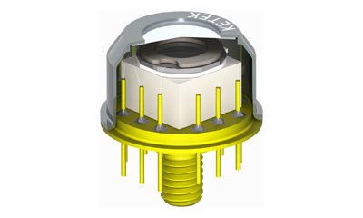
Development and manufacture of silicon drift detectors (SDD) and detector systems for material analysis – from wafer to module

KETEK GmbH
Munich (Hofer Str. 3) · Munich (Hansastraße 27c) · Neubiberg (Werner-Heisenberg-Weg 39) · Beijing, China (Sales Office)New on Amplifa
About KETEK
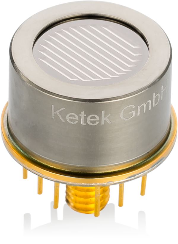
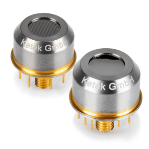
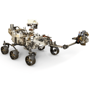
KETEK GmbH, headquartered in Munich, specializes in the development and manufacture of silicon drift detectors (SDD) used in energy-dispersive X-ray spectroscopy (EDS/EDX) and X-ray fluorescence analysis (XRF). The product portfolio covers the complete spectrum from high-purity silicon wafer to detector chip to finished, vacuum-encapsulated detector module in TO8 package, complemented by in-house developed analog and digital signal processing electronics such as preamplifiers (VIAMP), digital pulse processors (DPP3) and complete SDD systems (AXAS, ARRAY). Production takes place in a cleanroom environment using semiconductor planar technology with ion implantation and epitaxy; materials include high-purity silicon, ceramic chip carriers, graphene windows and beryllium windows. Customers come from electron microscopy, materials research, recycling/material sorting and food control; NASA Mars rovers such as Curiosity and Perseverance are equipped with KETEK detectors. The owner-managed company employs around 120 staff at sites in Munich, Neubiberg and a sales office in Beijing, serving customers worldwide.
- Site
- München
- Processes
- Semiconductor processing / chip manufacturing (planar technology, ion implantation, epitaxy), Manufacture of silicon drift detectors (SDD) – from wafer via detector chip to detector module, Development and manufacture of analog and digital signal electronics (preamplifier,, Production of graphene windows (CH: 1000 nm carbon without support grid; CL: 165 nm carbon, Cleanroom production (SDD production facility, cleanroom area doubled since 2011), Material analysis / elemental analysis using XRF & EDX (detectors for 0.05–30 keV, detection limit, Development and manufacture of silicon drift detectors (SDD) from wafer to detector module, In-house analog and digital signal processing electronics (preamplifier, digital pulse processor)
- Materials
- High-purity silicon (wafer), Graphene, Ceramic (chip carrier), Beryllium (window, 8 µm), Graphene window (CH/CL), Beryllium window (8 µm), Ceramic chip carrier, Planar technology / ion implantation / epitaxy
- Certificates
- ISO 9001:2015, ISO 9001
- Founded
- 1989
- Employees
- ~120
- Industries
- X-ray fluorescence spectrometry (XRF), Energy-dispersive X-ray spectroscopy (EDS/EDX), Electron microscopy (TEM), Material analysis and materials research, Recycling/material sorting, Food control (heavy metal detection)
- 01
Semiconductor processing (planar technology, ion implantation, epitaxy)
- 02
Detector chip manufacturing from silicon wafer
- 03
Graphene window production
- 04
Detector module assembly (chip carrier, Peltier cooling, vacuum encapsulation)
- 05
Manufacture of signal processing electronics
- 06
System integration and testing
- 07
Sales and support (including software/firmware)
Materials & Processes
High-purity silicon (wafer)
Base material for SDD chips, processed using planar technology with ion implantation and epitaxy.
Graphene window (CH/CL)
In-house developed carbon windows (CH: 1000 nm without support grid, CL: 165 nm with Si support grid) for improved transmission in the low-energy range.
Beryllium window (8 µm)
Classic single window for VITUS modules with large active area (H80/H150).
Ceramic chip carrier
Carrier material for mounting the SDD chip in the TO8 package.
Planar technology / ion implantation / epitaxy
Semiconductor processing methods used to manufacture the SDD chips in cleanroom production.
Sites
Munich (Hofer Str. 3)
DEHeadquarters: sales, development and manufacturing
- Materials
- Silicon, ceramic, graphene
- Cleanroom production (doubled area since 2011)
- SDD production facility
- Signal processing electronics manufacturing
Munich (Hansastraße 27c)
DEManufacturing and development of semiconductor detectors and detector systems
- Materials
- Silicon
Neubiberg (Werner-Heisenberg-Weg 39)
DEManufacturing and development of semiconductor detectors and detector systems
- Materials
- Silicon
Beijing (KETEK China)
CNSales office China
Components & Products
Inside the production
Industries
Processes & technical limits
| Processes | Tolerance | Max. part | Weight | Lot size | Materials |
|---|---|---|---|---|---|
| Semiconductor processing / chip manufacturing (planar technology, ion implantation, epitaxy)Engineering | – | – | – | – | Silicon |
| Manufacture of silicon drift detectors (SDD) – from wafer via detector chip to detector moduleAssembly | – | – | – | – | Silicon, Ceramic, Graphene |
| Development and manufacture of analog and digital signal electronics (preamplifier,Assembly | – | – | – | – | – |
| Production of graphene windows (CH: 1000 nm carbon without support grid; CL: 165 nm carbonEngineering | – | – | – | – | Graphene, Silicon, Carbon |
| Cleanroom production (SDD production facility, cleanroom area doubled since 2011)Engineering | – | – | – | – | – |
| Material analysis / elemental analysis using XRF & EDX (detectors for 0.05–30 keV, detection limitTesting | – | – | – | – | – |
7 Anlagen & Maschinen
| Machine | Manufacturer / model | Quantity | Working area | Year built | Site |
|---|---|---|---|---|---|
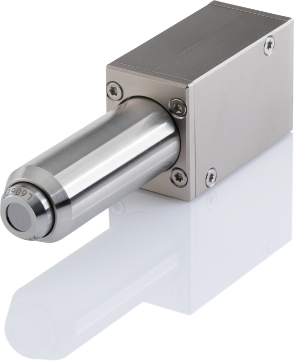
| Silicon drift detector (SDD) modules VITUS series | KETEK VITUS H7/H20/H20 SLF/H30/H50/K50/H80/H150 | – | 7–150 mm² collimated area | – | Munich |
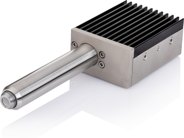
| Complete SDD systems (SDD + preamplifier + DPP3 + power supply) | KETEK AXAS-D 3.0 / AXAS-A 3.0 | – | – | 2024 | Munich |
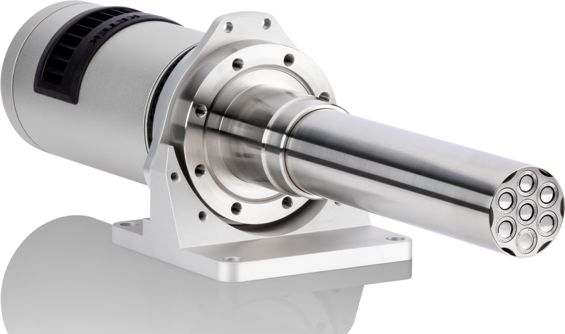
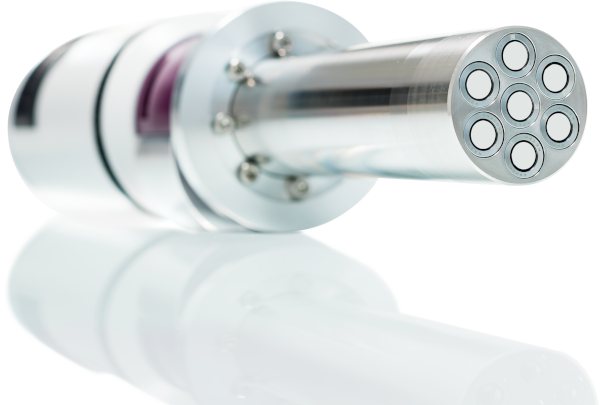
| Multi-channel SDD array (3–7 channels) | KETEK ARRAY 3.0 | – | up to 350 mm² collimated area (7-channel: 560 mm²) | 2024 | Munich |
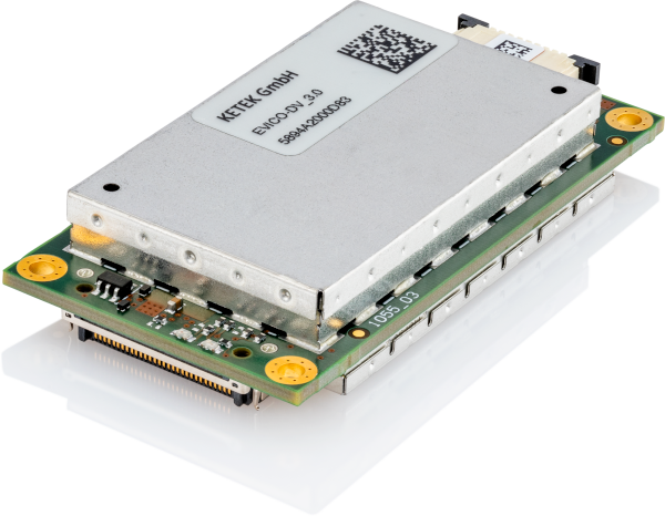
| OEM SDD electronics with DPP3 | KETEK VICO-DV 3.0 / VICO-AV 3.0 | – | – | 2023 | Munich |
| OEM preamplifier modules (SDD + preamplifier) | KETEK VIAMP-KC 3.0 / VIAMP-KL 3.0 / VIAMP-KP 3.0 | – | – | 2023 | Munich |
| Digital pulse processor | KETEK DPP3 (VICO-DP/DPP2) | – | – | 2015 | Munich |
| Peltier coolers (installed in SDD modules) | – | – | – | – | Munich |
Additional services
Reference customers
Quality
KETEK is certified to ISO 9001:2015 (TÜV SÜD, Reg. No. 12 100 33497 TMS) for sales, development and manufacturing of semiconductor detectors, detector systems, radiation sources and associated electronics. Process objectives are maximum yield, on-time delivery and error-free quality.
| Evidence | Munich (Hofer Str. 3) | Munich (Hansastraße 27c) | Neubiberg (Werner-Heisenberg-Weg 39) |
|---|---|---|---|
| ISO 9001 |
History
- 1989
Foundation of KETEK GmbH by Dr. Josef Kemmer
- 1995
First SDD generation; new management Silvia Wallner and Dr. Reinhard Fojt
- 2002
ISO 9001:2000 certification; product launch of the AXAS X-ray acquisition system
- 2005
Introduction of the VITUS SDD series
- 2007
Product launch of the VIAMP module (VITUS SDD + preamplifier)
- 2008
World record energy resolution: 120.9 eV for Mn Kα
- 2011
Doubling of cleanroom area at the Munich headquarters
- 2012
VITUS SDD on the Mars rover Curiosity; introduction of the VITUS CUBE SDD series; first SiPM modules
- 2013
Largest circular SDD with 150 mm² active area as a standard product
- 2015
Introduction of the Digital Pulse Processor DPP2 (VICO-DP)
- 2017
Introduction of a 7-channel SDD array with 560 mm² total collimated area
- 2018
In-house graphene window reaches market maturity
- 2019
VICO-DV 2.0 – smallest OEM SDD electronics
- 2020
AXAS-A/D 2.0 compact complete system presented
- 2021
VITUS 2.0 SDD generation; SDDs on the Mars rover Perseverance; sale of SiPM assets to Broadcom
- 2022
Low-Energy Graphene Window (CL) presented
- 2023
VICO-DV 3.0 with DPP3; VIAMP-KP 3.0 for vacuum applications
- 2024
ARRAY 3.0 (3–7 channels) and AXAS 3.0 with DPP3 introduced
- 2025
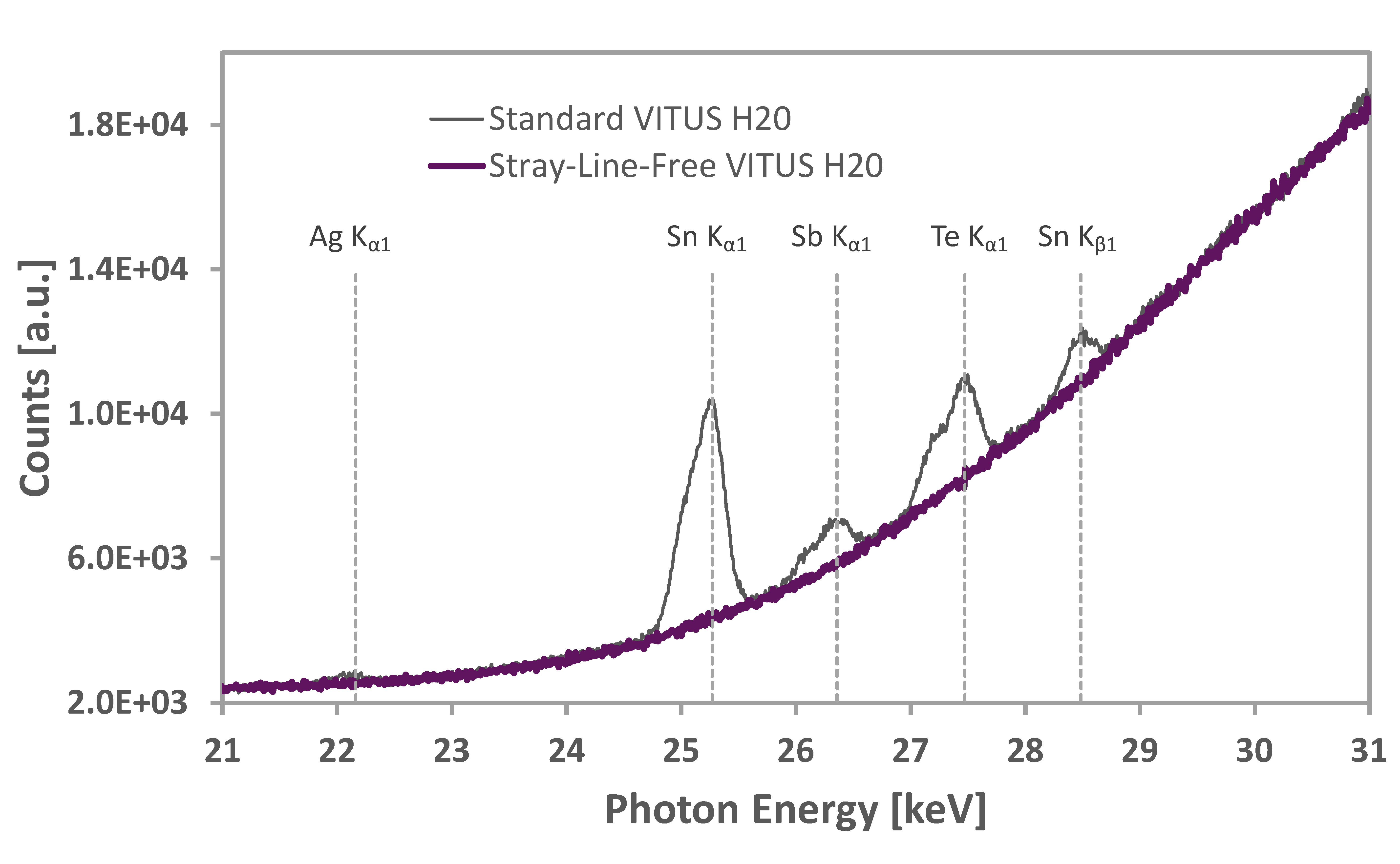
VITUS H20 SLF (Stray-Line-Free) SDD introduced