
Sales and system solutions for wafer handling, process automation and metrology in semiconductor and microelectronics manufacturing

KITEC microelectronic technologie GmbH
LübeckNew on Amplifa
About KITEC
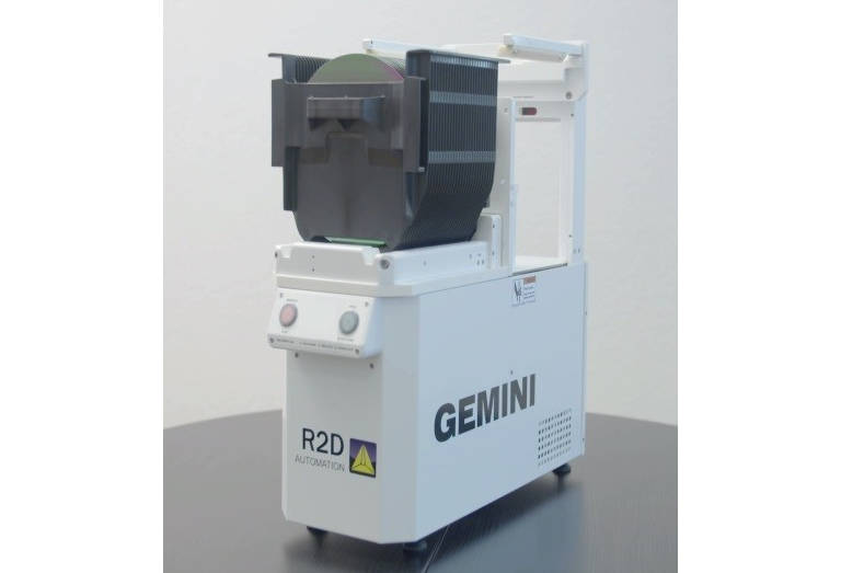
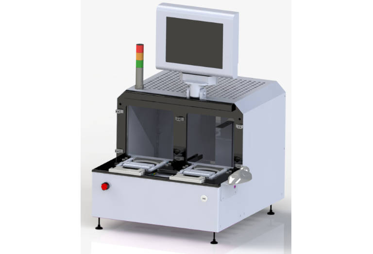
KITEC microelectronic technologie GmbH was founded in 1987 and offers equipment, systems and solutions for semiconductor production, thin-film and microelectronics technologies. The company operates as a distributor and manufacturer's representative for high-tech products and specializes in products for front-end wafer processing, wafer handling, metrology as well as general thin-film and flat panel display technologies. The portfolio includes wafer handling systems, wafer transfer systems, wafer sorters, wafer ID readers, vacuum wands as well as systems for wafer inspection, resistance and resistivity measurement (including the Gemini 300). KITEC supplies both complete systems and individual devices for specific requirements in handling, inspection, measurement and automation – manual, semi-automatic or automatic. The company supports customers in selecting systems according to wafer size, material, process and degree of automation. From Lübeck, KITEC serves customers across Europe and is connected to the US market.
- Site
- Lübeck
- Processes
- Non Contact Resistance and Resistivity Measurement, Metrology and Wafer Inspection, Wafer Edge Defect Inspection, Visual Wafer Inspection, Wafer Transfer Systems, Process Tool Automation, Wafer Handling, Wafer Transfer
- Materials
- Wafer Handling Systems, Wafer Transfer Systems, Metrology (Gemini 300), Process Tool Automation
- Founded
- 1987
- Industries
- Semiconductor industry, Microelectronics, Thin-film technologies, Flat Panel Display
- 01
Consulting on system selection (manual, semi-automatic, automatic)
- 02
Distribution / Manufacturer's Representation
- 03
Metrology and wafer inspection
- 04
Wafer handling and wafer transfer
- 05
Process automation
Products and Processes
Wafer Handling Systems
Systems for picking up, handling and positioning wafers in front-end processing.
Wafer Transfer Systems
Systems for automated transfer of wafers between process units.
Metrology (Gemini 300)
Non-contact measurement of resistance and resistivity as well as wafer inspection.
Process Tool Automation
Automation of process tools for semiconductor manufacturing.
Locations
Lübeck
DEHeadquarters, sales and consulting
- Materials
- Wafer Handling Systems, Wafer Sorter, Wafer ID Reader, Vacuum Wands, Wafer Transfer Systems, Metrology (Gemini 300)
- Wafer Handling Systems
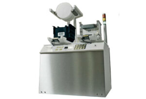
- Wafer Sorter
- Wafer ID Reader
- Vacuum Wands
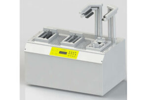
- Wafer Transfer Systems
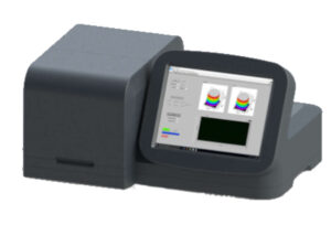
- Wafer Inspection / Metrology System Gemini 300
Systems and Devices
Inside the production

Industries
Processes & technical limits
| Processes | Tolerance | Max. part | Weight | Lot size | Materials |
|---|---|---|---|---|---|
| Non Contact Resistance and Resistivity MeasurementTesting | – | – | – | – | – |
| Metrology and Wafer InspectionTesting | – | – | – | – | – |
| Wafer Edge Defect InspectionTesting | – | – | – | – | – |
| Visual Wafer InspectionTesting | – | – | – | – | – |
| Wafer Transfer SystemsAssembly | – | – | – | – | – |
| Process Tool AutomationAssembly | – | – | – | – | – |
6 Anlagen & Maschinen
| Machine | Manufacturer / model | Quantity | Working area | Year built | Site |
|---|---|---|---|---|---|
| Wafer Handling Systems | – | – | – | – | Lübeck |
| Wafer Sorter | – | – | – | – | – |
| Wafer ID Reader | – | – | – | – | – |
| Vacuum Wands | – | – | – | – | – |
| Wafer Transfer Systems | – | – | – | – | – |
| Wafer Inspection / Metrology System | Gemini 300 | – | – | – | – |
Additional services
History
- 1987
Founding of KITEC microelectronic technologie GmbH for the distribution of equipment and consumables for semiconductor, thin-film and microelectronics technologies