KLA develops and manufactures process control and process solutions for semiconductor and electronics manufacturing – from inspection and metrology to etch and deposition.
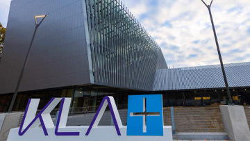
KLA Corporation
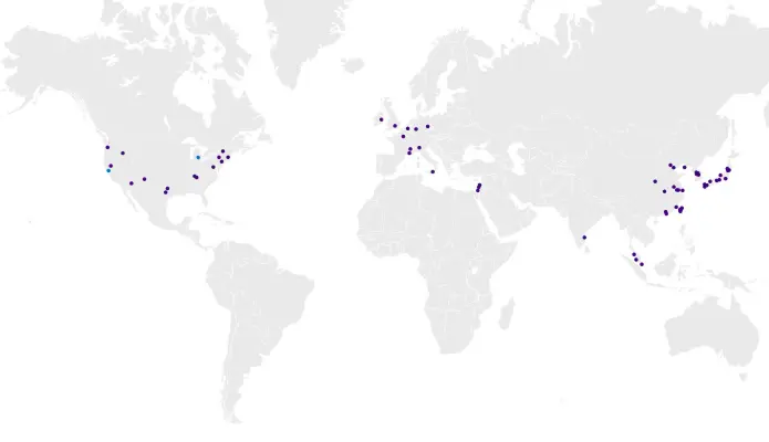
Milpitas (US) · Newport (GB) · Weilburg (DE) · Jena (DE) · Ann Arbor (US) · Migdal Ha'Emek (IL) · Yavne (IL) · Singapore (SG) · Shenzhen (CN) · San Diego (US)New on Amplifa
About KLA
KLA Corporation is a globally active supplier of process control and process-enabling solutions for semiconductor manufacturing. The company develops and manufactures defect-inspection systems, metrology systems, mask and reticle qualification systems, and process solutions such as plasma etch, physical vapor deposition (PVD) and plasma-enhanced chemical vapor deposition (PECVD). The portfolio is complemented by direct imaging systems and additive printing processes for printed circuit boards and IC substrates, film thickness reflectometers (Filmetrics), as well as software and computational analytics. The products are used across the board from research and development to high-volume manufacturing and process materials such as silicon wafers, GaN power semiconductors and AlScN thin films. Customers come from semiconductor manufacturing, wafer production, advanced packaging, PCB manufacturing, 5G, automotive, IoT, AI/data centers, solar energy and research. In addition to its headquarters in Milpitas (California), KLA maintains manufacturing and development sites including in Newport (Wales), Weilburg and Jena (Germany), Ann Arbor (Michigan), Israel, Singapore and Shenzhen. KLA is listed on the NASDAQ and employs around 16,000 people worldwide.
- Site
- Milpitas, CA, USA
- Processes
- Defect inspection and review (wafer/IC), Metrology / measurement systems (including Archer, SpectraShape, Aleris, Axion), Physical vapor deposition (PVD), SPTS Sigma, Plasma-enhanced CVD (PECVD), SPTS Delta/Osprey, Plasma etch (SPTS Omega, Mosaic, plasma dicing), UV laser drilling / Xactix Xe-etched (Xactix CVE/e2/X4), Direct imaging for PCB patterning and solder mask, Inkjet and additive printing (Orbotech Magna/Neos/Sprint)
- Materials
- Silicon wafers (semiconductor), GaN (gallium nitride) power semiconductors, AlScN (aluminum scandium nitride) / electrode metals for BAW filters, Silicon wafers, Gallium nitride (GaN), AlScN / electrode metals, Physical vapor deposition (SPTS Sigma), Plasma-enhanced CVD (SPTS Delta/Osprey)
- Certificates
- ISO 9001:2015, ISO 14001:2015, ISO 45001:2018, IATF 16949
- Founded
- 1976
- Employees
- ~16000
- Industries
- Semiconductor manufacturing, Wafer production, Reticle/mask qualification, Advanced packaging, PCB & IC substrates, 5G
- 01
R&D (electron/photon optics, sensor technology, AI)
- 02
Development of process solutions (etch, PVD, PECVD, direct imaging)
- 03
System manufacturing (including Newport cleanroom)
- 04
Qualification and testing (inspection, metrology)
- 05
Software and computational analytics
- 06
Service, upgrades and spare parts supply
Materials and Processes
Silicon wafers
Base material of semiconductor manufacturing, to which inspection, metrology as well as etch and deposition processes relate.
Gallium nitride (GaN)
Power semiconductor material for 5G and high-frequency applications, supported by dedicated etch and deposition processes.
AlScN / electrode metals
Thin-film material for advanced BAW filters, deposited with SPTS deposition systems.
Physical vapor deposition (SPTS Sigma)
Coating process for applying functional layers to wafers.
Plasma-enhanced CVD (SPTS Delta/Osprey)
Plasma-supported coating process for creating layers in wafer and packaging processes.
Plasma etch (SPTS Omega, Mosaic)
Etching processes for targeted material removal including plasma dicing for wafer separation.
Xenon difluoride / vapor etch (Xactix, Primaxx)
Gas-phase etching processes for selective, gentle material removal.
Direct imaging (Orbotech Diamond, Nuvogo)
Exposure processes for patterning and solder mask on printed circuit boards and IC substrates.
Locations
Milpitas, CA
USCorporate headquarters

Newport
GBManufacturing and R&D (SPTS division)
- Materials
- Wafer: etch, PVD, PECVD
- SPTS Sigma PVD
- SPTS Delta/Osprey PECVD
- SPTS Omega plasma etch
- Demo cleanroom ISO 7 / ISO 5
Weilburg
DEManufacturing and R&D (KLA MIE GmbH)
Jena
DEDevelopment, manufacturing, sales and service
Ann Arbor, MI
USManufacturing and R&D / growth center
Migdal Ha'Emek
ILDevelopment, manufacturing, sales and service
Yavne
ILManufacturing (Orbotech)
Singapore
SGManufacturing
Shenzhen
CNManufacturing
San Diego, CA
USFilmetrics headquarters
Products and Systems
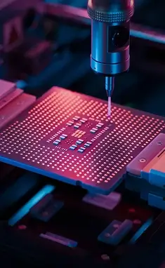

Inside the production


Industries
Processes & technical limits
| Processes | Tolerance | Max. part | Weight | Lot size | Materials |
|---|---|---|---|---|---|
| Defect inspection and review (wafer/IC)Testing | – | – | – | – | Semiconductor wafers, ICs |
| Metrology / measurement systems (including Archer, SpectraShape, Aleris, Axion)Testing | – | – | – | – | Semiconductor wafers |
| Physical vapor deposition (PVD), SPTS SigmaSurface | – | – | – | – | Semiconductor wafers |
| Plasma-enhanced CVD (PECVD), SPTS Delta/OspreySurface | – | – | – | – | Semiconductor wafers |
| Plasma etch (SPTS Omega, Mosaic, plasma dicing)Surface | – | – | – | – | Semiconductor wafers |
| UV laser drilling / Xactix Xe-etched (Xactix CVE/e2/X4)Surface | – | – | – | – | Semiconductor wafers |
| Direct imaging for PCB patterning and solder maskSurface | – | – | – | – | PCB, IC substrates |
| Inkjet and additive printing (Orbotech Magna/Neos/Sprint)Surface | – | – | – | – | PCB |
| PCB inspection, repair and imagingTesting | – | – | – | – | PCB |
| Film thickness measurement / reflectometry (Filmetrics)Testing | – | – | – | – | Thin films |
| Mask/reticle qualification (Teron, TeraScan)Testing | – | – | – | – | Reticles, Mask blanks |
12 Anlagen & Maschinen
| Machine | Manufacturer / model | Quantity | Working area | Year built | Site |
|---|---|---|---|---|---|
| PVD coating system | SPTS (KLA) Sigma PVD | – | – | – | Newport, Wales (UK) |
| PECVD coating system | SPTS (KLA) Delta PECVD / Osprey PECVD | – | – | – | Newport, Wales (UK) |
| MVCVD (MVD300/300E) | KLA MVD300/300E | – | – | – | – |
| Plasma etch system (ICP/Rapier/DSi-v/SynapsEtch) | SPTS (KLA) Omega | – | – | – | Newport, Wales (UK) |
| Plasma dicing system | SPTS (KLA) Mosaic / Rapier-S / Rapier-300S | – | – | – | – |
| Xenon difluoride etch system | Xactix (KLA) CVE / e2 / X4 | – | – | – | – |
| Vapor etch system | Primaxx (KLA) Monarch 25 / Monarch 3 / Monarch 300 / uEtch | – | – | – | – |
| Defect inspection systems | KLA Surfscan / 39xx / 29xx / CIRCL / Voyager / eDR7380 | – | – | – | – |
| Measurement/metrology systems | KLA Archer / SpectraShape / Aleris / Axion / Candela | – | – | – | – |
| Direct imaging systems | Orbotech (KLA) Diamond 10/10W / Nuvogo / Serena / Corus / Infinitum | – | – | – | – |
| Film thickness reflectometer | Filmetrics (KLA) F10/F20/F3/F32/F40/F50/F54/F60 | – | – | – | San Diego, CA |
| Mask/reticle inspection system | KLA Teron 6xx / TeraScan 5xx | – | – | – | – |
Additional services
Quality and Certification
KLA is certified to ISO 9001:2015 (DNV) and operates cleanroom manufacturing in Newport (ISO 7 and ISO 5). In addition, certified environmental (ISO 14001:2015) and occupational health and safety management systems (ISO 45001:2018) apply.
| Evidence | Milpitas | Newport | Weilburg | Jena |
|---|---|---|---|---|
| ISO 9001:2015 | ||||
| ISO 14001:2015 | ||||
| ISO 45001:2018 | ||||
| IATF 16949 |
History
- 1975
Pioneering mask inspection system; the beginning of the era of semiconductor process control
- 1976
Founding of KLA; since then supporting yield improvement through process control
- 1984
SPTS (Wales) begins innovating in the semiconductor equipment sector
- 2019
Acquisition of SPTS (etch/deposition) and Orbotech
- 2025
Opening of the new R&D and manufacturing center in Newport, Wales (USD 138 million)
- 2026
50 years of innovation and customer success; celebration with the NASDAQ bell