
International technology group for lithography, 3D microprinting, wafer processing and analytics technology for micro- and nanofabrication.

LAB14 GmbH
Heidelberg · 28 sites in Europe, America and AsiaNew on Amplifa
About LAB14
LAB14 GmbH is an international technology group headquartered in Heidelberg, specializing in micro- and nanotechnology. The group brings together highly specialized subsidiaries with complementary expertise in fabrication, structuring, analysis and metrology. The portfolio includes maskless direct-write lithography and photomask systems (Heidelberg Instruments), 3D microprinting based on two-photon polymerization (Nanoscribe), software for process optimization (GenISys), industrial inkjet printing systems and precision photolithography (Notion Systems), surface analysis and atomic force microscopy (SPECSGROUP, Nanosurf), as well as wafer processing systems for coating, cleaning and etching plus chiller and heat exchange systems (Amcoss). The technologies serve semiconductor manufacturing, MEMS, micro-optics, sensors, displays, aerospace, life sciences and materials research. With more than 1,200 employees, 28 sites in Europe, America and Asia, and more than 2,300 customers, LAB14 is part of RSBG SE and thus of the RAG Foundation.
- Site
- Heidelberg
- Processes
- Maskless direct-write lithography (micro/nano patterning, 2D and 2.5D grayscale lithography), Photomask fabrication (lithography equipment for high-volume production), 3D microprinting / two-photon polymerization (additive manufacturing on the nano, micro and meso, Grayscale lithography systems, Software for process optimization in micro/nano fabrication (lithography, data modeling, metrology), Precision photolithography, Industrial inkjet printing (additive electronics for electronics, displays, semiconductors), Inkjet printing for displays, PCBs, semiconductors and optical 3D components
- Materials
- Specially developed printing materials for microfabrication, Two-Photon Polymerization, Maskless Direct-Write Lithography, Industrial Inkjet Printing, Surface Nanoanalysis (XPS), Atomic Force Microscopy (AFM), Wafer Processing
- Certificates
- ISO 9001
- Founded
- 2022
- Employees
- 1200+
- Industries
- Semiconductor manufacturing, MEMS, Micro-optics, Photomasks, Sensors, Display and electronics industry
- 01
Engineering and software for process optimization
- 02
Maskless direct-write lithography / photomask fabrication
- 03
3D microprinting (two-photon polymerization)
- 04
Industrial inkjet printing / additive electronics
- 05
Wafer coating, cleaning and etching
- 06
Surface analysis and metrology (AFM, XPS)
- 07
Maintenance, cleaning and repair (vacuum technology, cleanroom)
- 08
Service, training, spare parts and process management software
Technologies and Processes
Two-Photon Polymerization
Additive 3D microfabrication of high-precision structures on the nano, micro and meso scales using specially developed printing materials.
Maskless Direct-Write Lithography
2D and 2.5D grayscale patterning for photomasks, MEMS, micro-optics, packaging and sensors.
Industrial Inkjet Printing
Additive electronics for electronics, displays, PCBs, semiconductors and optical 3D components.
Surface Nanoanalysis (XPS)
Analysis of surfaces under vacuum conditions for materials research and nanotechnology.
Atomic Force Microscopy (AFM)
Precision measuring platforms for life sciences, materials research and industry.
Wafer Processing
Coating, cleaning and etching systems as well as customized chillers and heat exchangers for the semiconductor industry.
Sites and Subsidiaries
Heidelberg
DEHeadquarters of LAB14 GmbH
Eggenstein-Leopoldshafen
DENanoscribe – development and production of 3D printing and grayscale lithography systems (KIT spin-off)
- Materials
- Specially developed printing materials
- 3D printing systems (two-photon polymerization)
Schwetzingen
DENotion Systems – headquarters, industrial inkjet printing systems and precision photolithography
- Industrial inkjet printing systems
Singen
DENotion Systems – additional site
- Industrial inkjet printing systems
Austria (Amcoss)
DEAmcoss GmbH – wafer processing systems (coating, cleaning, etching) and chillers/heat exchangers
- Wafer processing systems
- Chillers and heat exchangers
Switzerland (Nanosurf)
DENanosurf AG – development and manufacture of atomic force microscopes
- Atomic force microscopes (AFM)
Munich (GenISys)
DEGenISys GmbH – software for process control in micro- and nanofabrication
- Process management software
Grenoble (40-30)
DE40-30 SAS – maintenance, cleaning and repair in vacuum technology, electronics and cleanrooms
- Process management software
Inside the production

Industries
Processes & technical limits
| Processes | Tolerance | Max. part | Weight | Lot size | Materials |
|---|---|---|---|---|---|
| Maskless direct-write lithography (micro/nano patterning, 2D and 2.5D grayscale lithography)Engineering | – | – | – | – | – |
| Photomask fabrication (lithography equipment for high-volume production)Engineering | – | – | – | – | – |
| 3D microprinting / two-photon polymerization (additive manufacturing on the nano, micro and mesoAdditive | – | – | – | – | specially developed printing materials |
| Grayscale lithography systemsAdditive | – | – | – | – | – |
| Software for process optimization in micro/nano fabrication (lithography, data modeling, metrology)Engineering | – | – | – | – | – |
| Precision photolithographyEngineering | – | – | – | – | – |
| Industrial inkjet printing (additive electronics for electronics, displays, semiconductors)Additive | – | – | – | – | – |
| Inkjet printing for displays, PCBs, semiconductors and optical 3D componentsAdditive | – | – | – | – | – |
| Surface analysis (XPS analysis, surface analysis under vacuum conditions)Testing | – | – | – | – | – |
| Atomic force microscopy (AFM) for life sciences, materials research and industryTesting | – | – | – | – | – |
| Maintenance, cleaning and repair in vacuum technology, electronics and cleanroom environmentsSurface | – | – | – | – | – |
| Wafer coatingSurface | – | – | – | – | Wafer |
| Wafer cleaningSurface | – | – | – | – | Wafer |
| Wafer etchingSurface | – | – | – | – | Wafer |
| Manufacture of cooling and heat exchange systems (chillers, heat exchangers)Engineering | – | – | – | – | – |
9 Anlagen & Maschinen
| Machine | Manufacturer / model | Quantity | Working area | Year built | Site |
|---|---|---|---|---|---|
| Direct-write lithography systems (benchtop systems up to high-end photomask systems) | Heidelberg Instruments | 1,500+ | – | – | – |
| 3D printing systems (two-photon polymerization) | Nanoscribe | – | – | – | Eggenstein-Leopoldshafen (KIT spin-off) |
| Industrial inkjet printing systems | Notion Systems | – | – | – | Schwetzingen and Singen, Germany |
| Atomic force microscopes (AFM) | Nanosurf | – | – | – | Switzerland |
| Surface nanoanalysis systems | SPECS | – | – | – | – |
| Wafer processing systems (coating, cleaning, etching) | Amcoss | – | – | – | Austria |
| Chillers and heat exchangers | Amcoss | – | – | – | Austria |
| Automated analysis and metrology tools | Enviro (SPECSGROUP) | – | – | – | – |
| Scanning probe and transport measurement electronics | Nanonis (SPECSGROUP) | – | – | – | – |
Additional services
Reference customers
Quality
The LAB14 group supports quality assurance through leading metrology and analysis technology from its subsidiaries, including atomic force microscopy (Nanosurf), XPS surface analysis under vacuum conditions (SPECS) and automated analysis and metrology tools (Enviro). Amcoss, as a subsidiary, is ISO 9001 certified.
| Evidence | Austria (Amcoss) |
|---|---|
| ISO 9001 |
History
- 2019
Founding of RSBG Advanced Manufacturing Technologies GmbH (RSBG AMT), one of five clusters of RSBG SE
- 2022
Founding of LAB14 GmbH as a subsidiary of RSBG SE (part of the RAG Foundation); renamed from RSBG AMT
- 2023
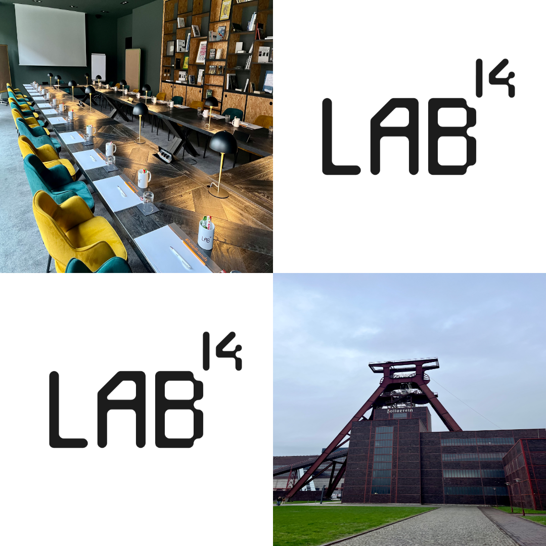
LAB14 Strategy and Technology Meeting in Essen with a guided tour of the Zeche Zollverein and a presentation on the history of the RAG Foundation
- 2024
December: Nanoscribe joins the LAB14 group as a new subsidiary
- 2025
July: Announcement of the merger of Osiris International and Notion Systems; the company name remains Notion Systems
- 2026
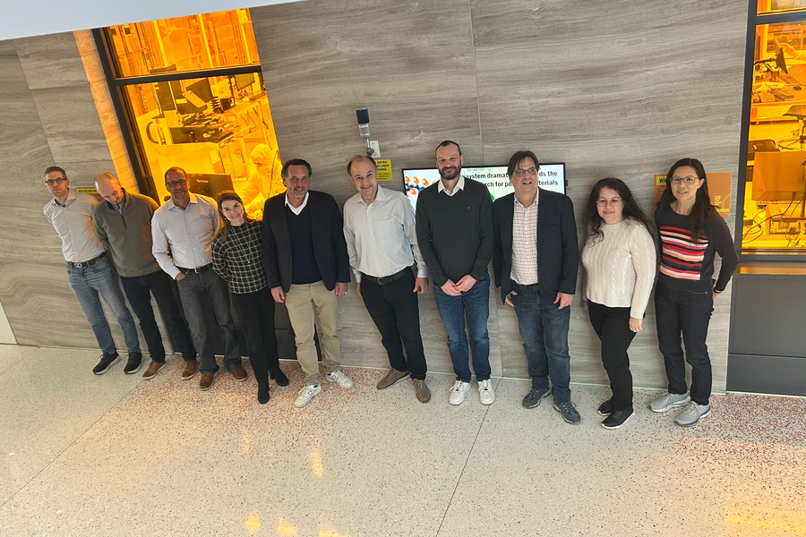
March: LAB14 joins the MIT.nano Consortium
- 2026
October 1: New management board – Thomas Wiedermann becomes Chief Change Officer, Martin Wynaendts van Resandt becomes Non-Executive Chairman