Femtosecond laser-based micro and nano manufacturing: 2PP systems, fs-laser processing, ion traps, EUV sources and ultrapure nanoparticles

Laser nanoFab GmbH
Hanover (labor and delivery address) · Garbsen (registered office)New on Amplifa
About Laser nanoFab
Laser nanoFab GmbH, based in Hanover, specializes in laser-based micro and nanotechnology. The company develops and manufactures systems and components using femtosecond lasers, including micro- and nanostructuring systems for two-photon polymerization (2PP) with structure sizes below 100 nm, fs-laser processing systems for subtractive ablation, and a debris-free EUV source based on microfocus X-ray tube technology. In addition, ultrapure precious-metal nanoparticles (femtoInk) and its own photoresist series (femtoBond) are offered. Services include process and system development, feasibility studies, process scale-up and custom systems for microtechnology. Application areas covered include quantum technologies (ion traps), EUV metrology, microfluidics, micro-optics, micromechanics as well as biology and medicine up to tissue engineering. The laboratory and goods receiving are located in Hanover, while the registered office is in neighboring Garbsen.
- Site
- Hannover
- Processes
- Two-photon polymerization (2PP), Stereolithography, Ultrashort pulse laser ablation (fs-laser processing), Replication process, Process development of laser-based processes for microtechnology, System development / custom systems for microtechnology, Process development for laser-based micro and nanotechnology (fs lasers), System development: custom systems for microtechnology
- Materials
- femtoBond 4B photoresist, femtoBond 4C photoresist, femtoInk - ultrapure precious-metal nanoparticles, Rogers material (ion trap chips), Gold (ion trap coating), Two-photon polymerization, Ultrashort pulse laser ablation, Stereolithography
- Industries
- Quantum technologies, EUV metrology, Microfluidics, Biology/Medicine (Tissue Engineering), Micro-optics, Micromechanics
- 01
CAD design and feasibility study
- 02
Process development with fs lasers
- 03
Additive manufacturing (2PP, stereolithography)
- 04
Subtractive manufacturing (fs-laser ablation)
- 05
Replication processes
- 06
System integration of custom systems
- 07
Testing and delivery
Materials and Processes
femtoBond 4B photoresist
Negative photoresist for two-photon polymerization with near-infrared lasers, e.g. around 800 nm.
femtoBond 4C photoresist
Negative photoresist for 2PP with green laser light, e.g. around 520 nm.
Two-photon polymerization
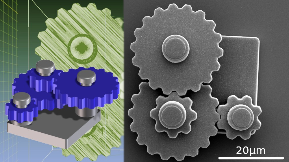
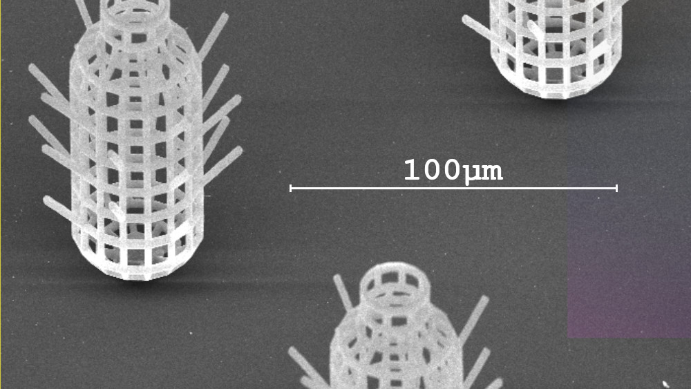
Direct laser writing of three-dimensional micro- and nanostructures with resolution down to below 100 nm.
Ultrashort pulse laser ablation
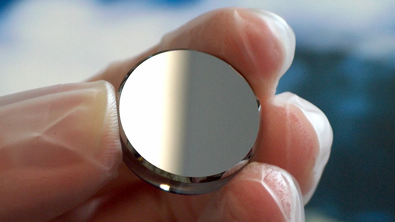
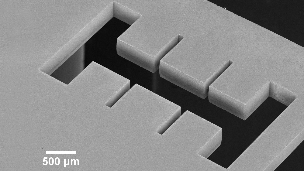
Subtractive machining of optical materials with femtosecond lasers.
Stereolithography
Additive manufacturing of structures from photoresists.
Replication process
Replication of microstructures from photoresists and biocompatible materials.
Gold
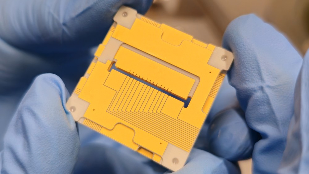
Coating of microstructured RF chips for ion traps.
Ultrapure precious-metal nanoparticles
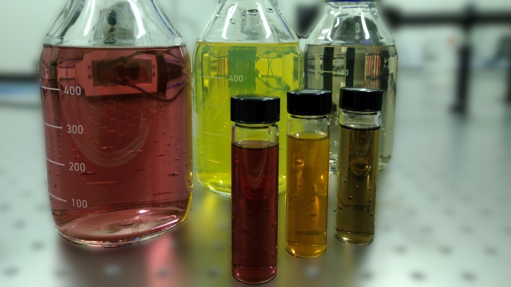
Production of ultrapure nanoparticles from precious metals.
Locations
Hanover
DELaboratory and delivery address, manufacturing and development
- Part weight / size
- 2PP build volume 10 × 10 × 10 cm; components up to 100 mm
- Lot size
- Prototypes and research orders
- Materials
- Photoresists (femtoBond), optical materials, biocompatible materials, gold, Rogers material, precious metals
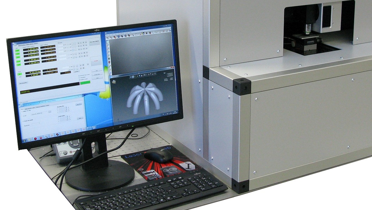
- M 4D micro- and nanostructuring system for 2PP (build volume 10×10×10 cm, footprint approx. 1 m²)
- A 4D fs-laser processing system
- Femtosecond pump laser (1030 nm, 10 W, 290 fs–10 ps)
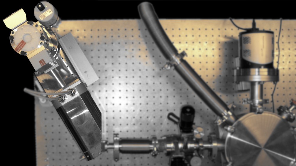
- EUV T2 - debris-free EUV source (microfocus X-ray tube technology)
Garbsen
DERegistered office and billing address
Components and Systems
Inside the production


Industries
Processes & technical limits
| Processes | Tolerance | Max. part | Weight | Lot size | Materials |
|---|---|---|---|---|---|
| Two-photon polymerization (2PP)Additive | – | 100 mm × 100 mm × 100 mm | – | – | Photoresists (femtoBond), Standard photoresists for lithography, biodegradable and biocompatible photoresists |
| StereolithographyAdditive | – | – | – | – | Photoresists |
| Ultrashort pulse laser ablation (fs-laser processing)Surface | – | – | – | – | Optical materials |
| Replication processPlastics | – | – | – | – | Photoresists, optical materials, biocompatible materials |
| Process development of laser-based processes for microtechnologyEngineering | – | – | – | – | – |
| System development / custom systems for microtechnologyEngineering | – | – | – | – | – |
4 Anlagen & Maschinen
| Machine | Manufacturer / model | Quantity | Working area | Year built | Site |
|---|---|---|---|---|---|
| 2PP micro- and nanostructuring system | Laser nanoFab GmbH M 4D | – | 10 cm x 10 cm x 10 cm (build volume), footprint approx. 1 m² | – | Hanover |
| fs-laser processing system | Laser nanoFab GmbH A 4D | – | – | – | Hanover |
| Femtosecond pump laser (1030 nm, 10 W, 290 fs-10 ps) | – | – | – | – | Hanover |
| EUV source (microfocus X-ray tube technology) | Laser nanoFab GmbH EUV T2 | – | – | – | Hanover |
Additional services