Development and sales of inspection and measurement systems for the semiconductor industry, including EUV mask inspection systems

Lasertec Corporation
Yokohama (Shin-Yokohama) · Düsseldorf · San José · Hwaseong/Pyeongtaek/Cheonan · Hsinchu/Tainan/Taichung · Shanghai/Nanjing/Beijing/Xiamen/Tianjin/Shenzhen · Singapore · Kildare · Kiryat GatNew on Amplifa
About Lasertec
Lasertec Corporation is a Japanese company headquartered in Yokohama that specializes in the development, manufacture and sale of inspection and measurement systems. The products are used mainly in the semiconductor industry for quality inspection of EUV masks, wafers and photolithographic photomasks. In addition, Lasertec offers inspection systems for photomasks in flat panel display (FPD) production as well as laser microscopes. The company was founded in 1960 as Tokyo ITV Laboratory and began with the development of X-ray cameras for medical special machines before expanding into the semiconductor industry in the 1970s. Lasertec pursues a fabless strategy and outsources manufacturing to subcontractors, allowing it to focus on research and development. In 2017, Lasertec was the first company worldwide to offer a commercial inspection system for EUV masks; in this niche the company is the global market leader. In addition to its headquarters in Yokohama, Lasertec maintains subsidiaries and branch offices in the USA, Germany, South Korea, Taiwan, China, Singapore, Ireland and Israel. The shares are listed on the Tokyo Stock Exchange and are part of the Nikkei 225.
- Site
- 222-8552 Yokohama, Kanagawa
- Processes
- Development, manufacture, sale and service of semiconductor inspection systems, FPD inspection systems, Laser microscopes
- Materials
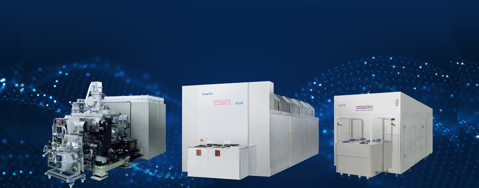
- EUV mask inspection systems, Wafer inspection systems, FPD inspection systems, Laser microscopes
- Founded
- 1960 (創業
- Industries
- Semiconductor industry, Flat Panel Display (FPD), Laser technology/Metrology, Medical technology (historical, X-ray cameras)
- 01
Research & Development
- 02
System design
- 03
Manufacturing by subcontractors (fabless)
- 04
Assembly & Integration
- 05
Sales and service worldwide
Technologies & Systems
EUV mask inspection systems
Inspection systems for quality control of EUV photomasks for extreme ultraviolet lithography.
Wafer inspection systems
Measurement and inspection systems for verifying the production readiness of semiconductor wafers.
FPD inspection systems
Inspection systems for photomasks in flat panel display production.
Laser microscopes
Laser-based microscopes for analytical and inspection applications.
Locations

Yokohama (Shin-Yokohama)
JPHeadquarters and R&D (Lasertec Innovation Park announced)
- Materials
- Semiconductor and FPD inspection systems, laser microscopes
Düsseldorf
DEBranch office since 1980
San José
USLasertec U.S.A., Inc. (since 1986); further locations in California, Oregon, New York, Idaho, North Carolina, Texas,
Products & Systems
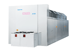
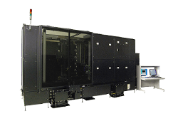
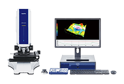
Inside the production

Industries
Additional services
Reference customers
History
- 1960
Founded as Tokyo ITV Laboratory; started with X-ray cameras for medical special machines
- 1970er
Expansion into inspection systems for photolithography in the semiconductor industry
- 1979
Opening of a branch office in San Mateo (USA)
- 1980
Opening of a branch office in Düsseldorf
- 1986
Renamed to Lasertec Corporation; founding of Lasertec U.S.A., Inc. in San José
- 2004
Stock exchange listing on Jasdaq
- 2012
Second listing on the Tokyo Stock Exchange
- 2017
Presentation of the world's first commercial inspection system for EUV masks
- 2020
Won the Intel annual supplier award
- 2022
Announcement of the Lasertec Innovation Park in Yokohama as a new R&D center
- 2024
Tetsuya Sendoda becomes Representative Director and President