Manufacturing of precision optics and optical coatings for laser applications from VUV (130 nm) to NIR (~7 µm)

LAYERTEC GmbH
MellingenNew on Amplifa
About LAYERTEC
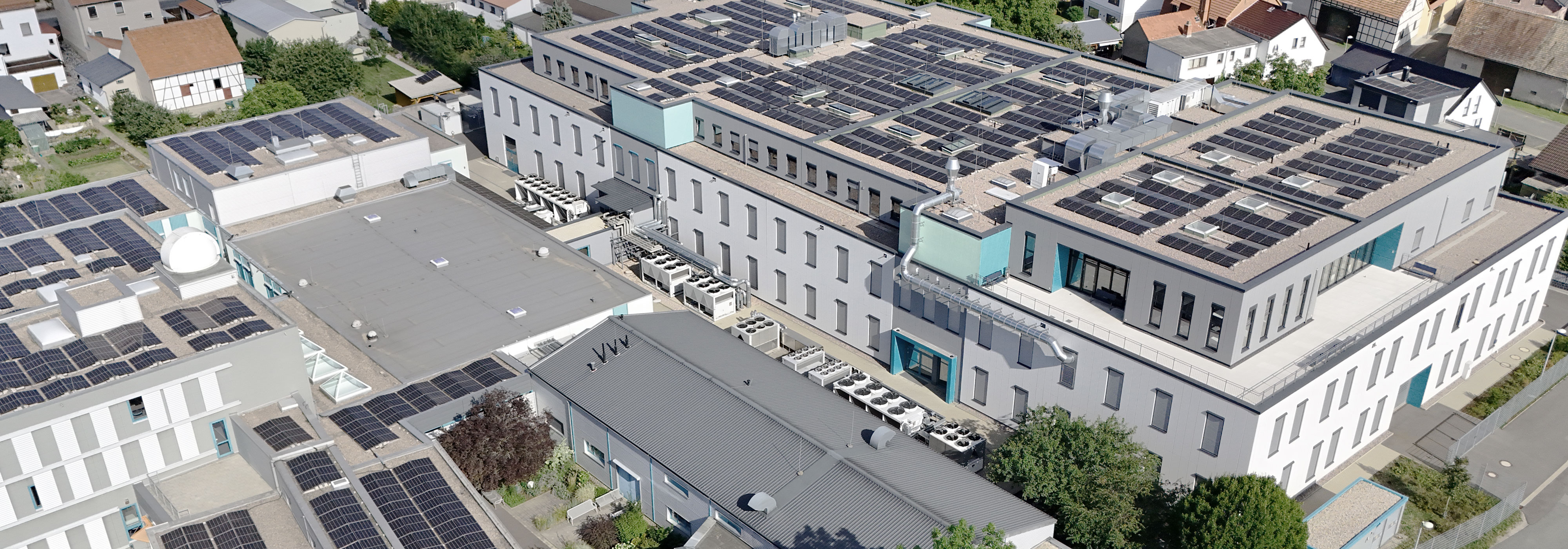
LAYERTEC GmbH was founded in 1990 as the first spin-off of Friedrich Schiller University Jena and produces optics of the highest quality for laser applications in the wavelength range from VUV (130 nm) to NIR (~7 µm). The company combines high-precision optics manufacturing (grinding, polishing, cleaning) with a wide range of advanced coating systems, including magnetron sputtering, ion beam sputtering (IBS), thermal and electron beam evaporation as well as ion-assisted deposition (IAD). With around 400 employees and 45 coating systems in Mellingen, mirror substrates, lenses, prisms, large optics up to 2000 mm edge length as well as optical and optomechanical assemblies are manufactured. Substrate materials include fused silica, N-BK7, ULE, Zerodur as well as crystals such as calcium fluoride, sapphire and YAG. Customers include industry, universities and research institutions, among others from laser research, medical technology, machine tool engineering and semiconductor manufacturing – from prototypes and small series for research institutions to series products for major customers (around 229,700 parts or ~4,500 different components per year, ~500 customers). In addition, special processes such as lithography, laser marking, solderable coatings and activation/bonding technologies are offered.
- Site
- Mellingen
- Processes
- Precision optics manufacturing (grinding, polishing, cleaning of mirror substrates, lenses, prisms), Magnetron sputtering (optical coatings), Ion beam sputtering (IBS), Thermal and electron beam evaporation (vacuum-based evaporation), Ion-assisted deposition (IAD, ion sources APS pro / LION), Zonal polishing (correction of planar surfaces, asphere manufacturing), Ultrasonic drilling/machining of glass substrates (e.g. conical bores), Ultrasonic cleaning (automated, coated and uncoated substrates)
- Materials
- Fused Silica (Corning 7980, Suprasil 300/3001/3002, Corning 7979, SQ1 E-193, SQ1 E-248, Infrasil, ULE, Zerodur, N-BK7, Calcium Fluoride (CaF2), Sapphire, YAG (undoped), Silicon (substrate material)
- Certificates
- NAThüringen (Sustainability Agreement Thuringia), berufundfamilie, ISO 9001, EN 9100
- Founded
- 1990
- Employees
- ~400
- Industries
- Laser research, Medical technology, Machine tool engineering, Semiconductor manufacturing, Quantum technology, Laser-controlled fusion
- 01
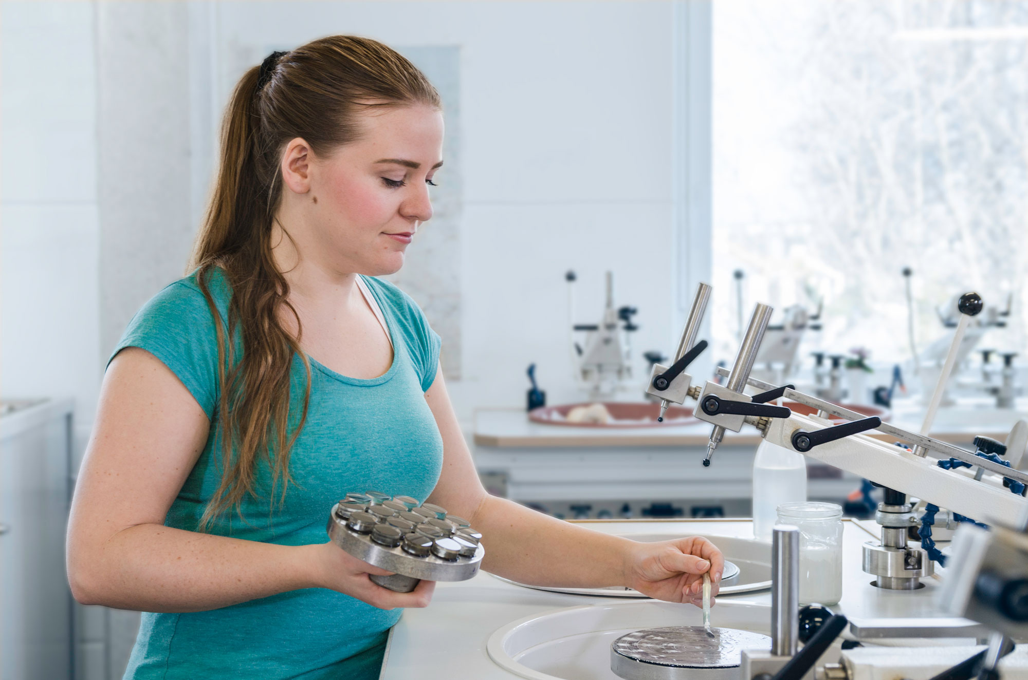
Substrate production (grinding, zonal polishing)
- 02
Ultrasonic cleaning
- 03
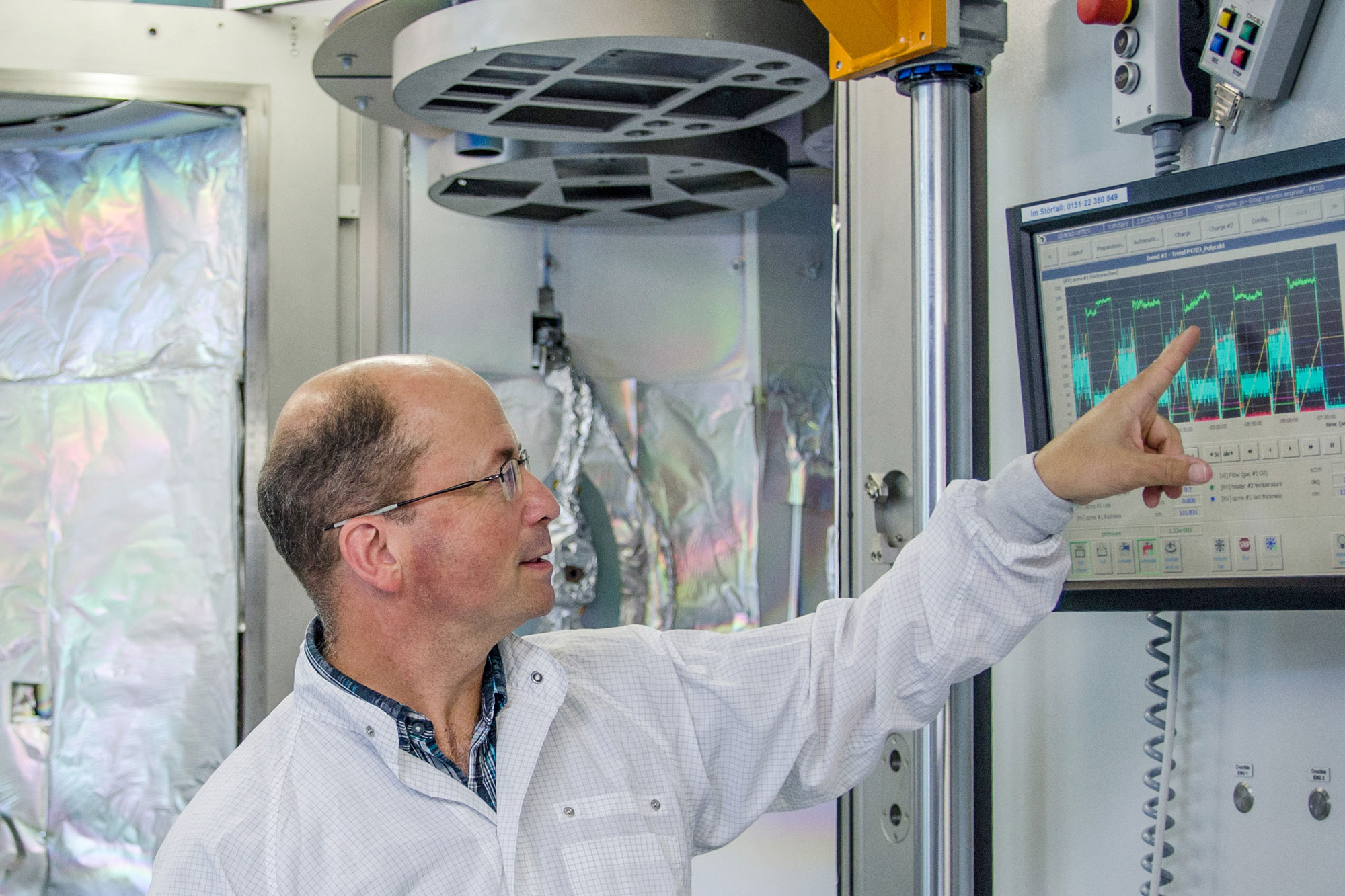
Coating (magnetron/ion beam sputtering, evaporation, IAD)
- 04
Special processes (lithography, laser engraving, joining/bonding)
- 05
Metrology and testing
- 06
Packaging and shipping
Materials and Processes
Fused Silica (Corning 7980, Suprasil 300/3001/3002, Infrasil 302, SQ1)
Standard material for mirror substrates, lenses and prisms from UV to IR with roughness < 0.2 nm.
ULE
Glass ceramic with extremely low thermal expansion for large optics and high-precision mirror substrates.
Zerodur
Thermally stable glass ceramic substrate for planar precision components.
N-BK7
Standard optical glass for lenses, prisms and mirror substrates in the visible spectral range.
Calcium Fluoride (CaF2)
Single-crystal material with a broad transmission range, mainly for UV optics and chromatic correction.
Sapphire (C-cut)
Hard single-crystal substrate for demanding optical applications.
YAG (undoped)
Single-crystal substrate for optics in the field of high-energy lasers.
Silicon
Substrate material for IR optics and metal-dielectric systems.
Magnetron Sputtering
Dense, low-scatter and durable coatings of oxides, fluorides and metals for substrates up to 60 cm diameter.
Ion Beam Sputtering (IBS)
Extremely low-absorption precision layers for substrates up to 30 cm diameter.
Thermal and Electron Beam Evaporation
Proven evaporation processes primarily for UV applications, also for cylindrical lenses up to 1.15 m length.
Ion-Assisted Deposition (IAD, APS pro / LION)
Dense, environmentally stable layers with a high laser damage threshold, including for large optics and line-beam optics.
Locations
Mellingen
DEHeadquarters with production of precision optics and optical coatings
- Part weight / size
- Optics up to 2000 mm edge length, substrates Ø 3–600 mm
- Lot size
- One-off pieces/prototypes to large series (~229,700 parts/year)
- Materials
- Fused silica, ULE, Zerodur, N-BK7, CaF2, sapphire, YAG, Si; oxides, fluorides, metals as coating materials
- 45 coating systems (sputtering, evaporation, IAD)
- More than 36 magnetron/IBS sputtering systems
- Inline sputtering system for substrates up to ~600 mm
- 7 vacuum coating systems (APS pro, LION)
- Automated ultrasonic cleaning systems
- CRD measuring stations for reflectivity/transmissivity
- PCI absorption measuring stations
- Automated defect inspection system according to ISO 10110
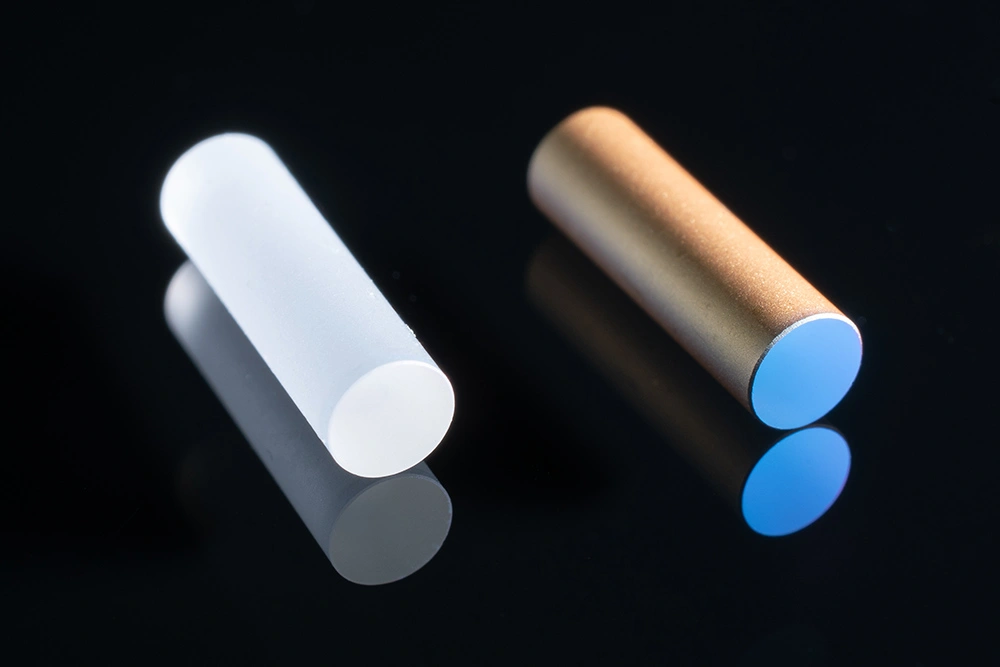
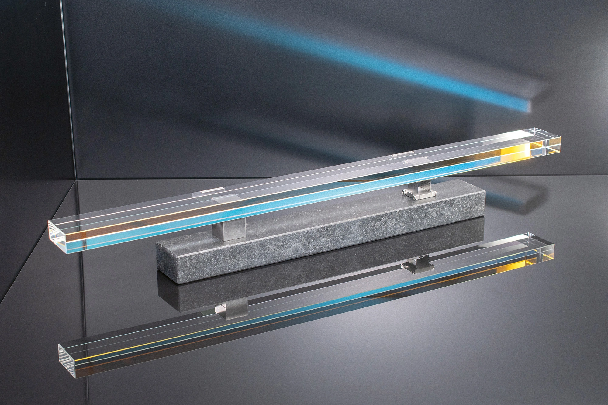
Components
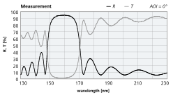
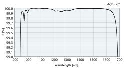
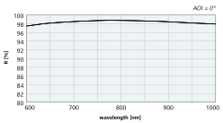
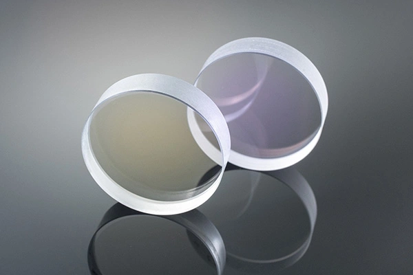
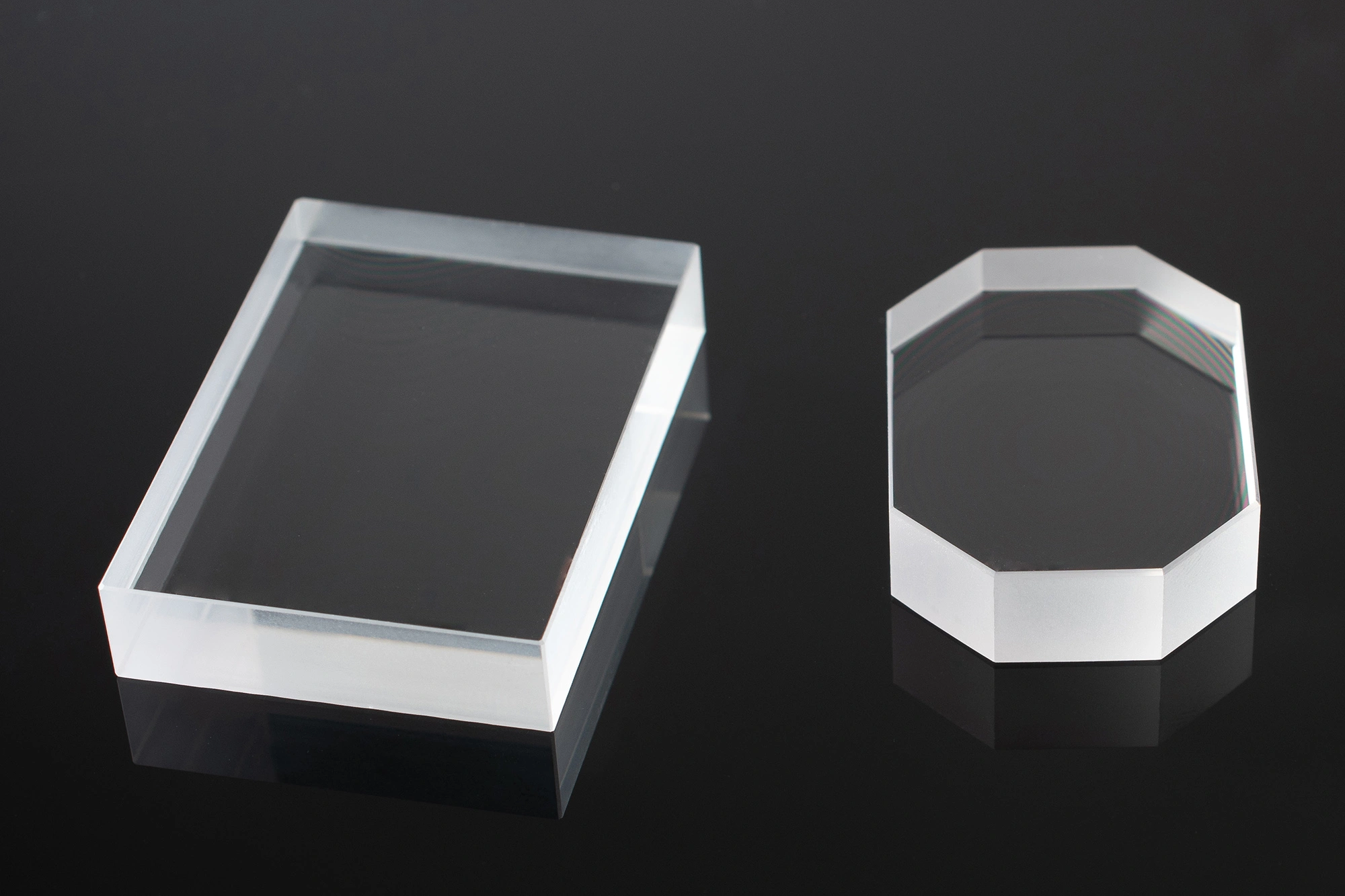
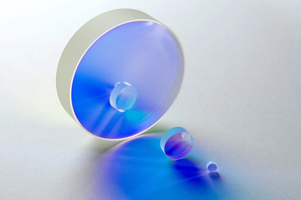
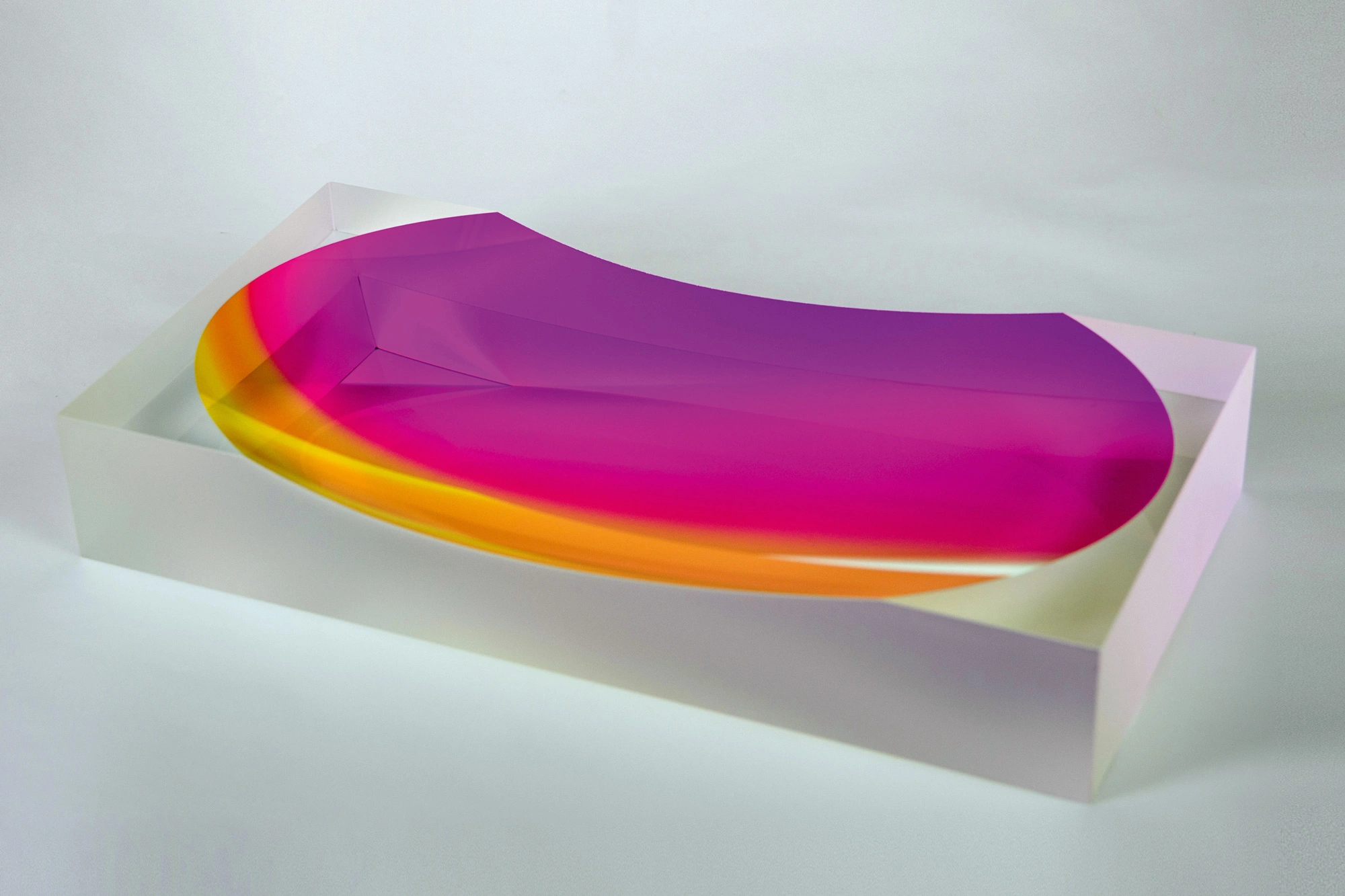
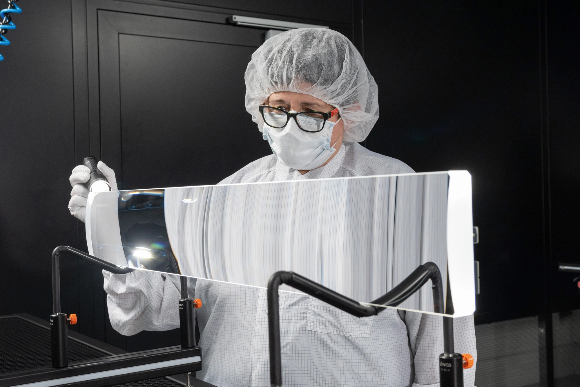
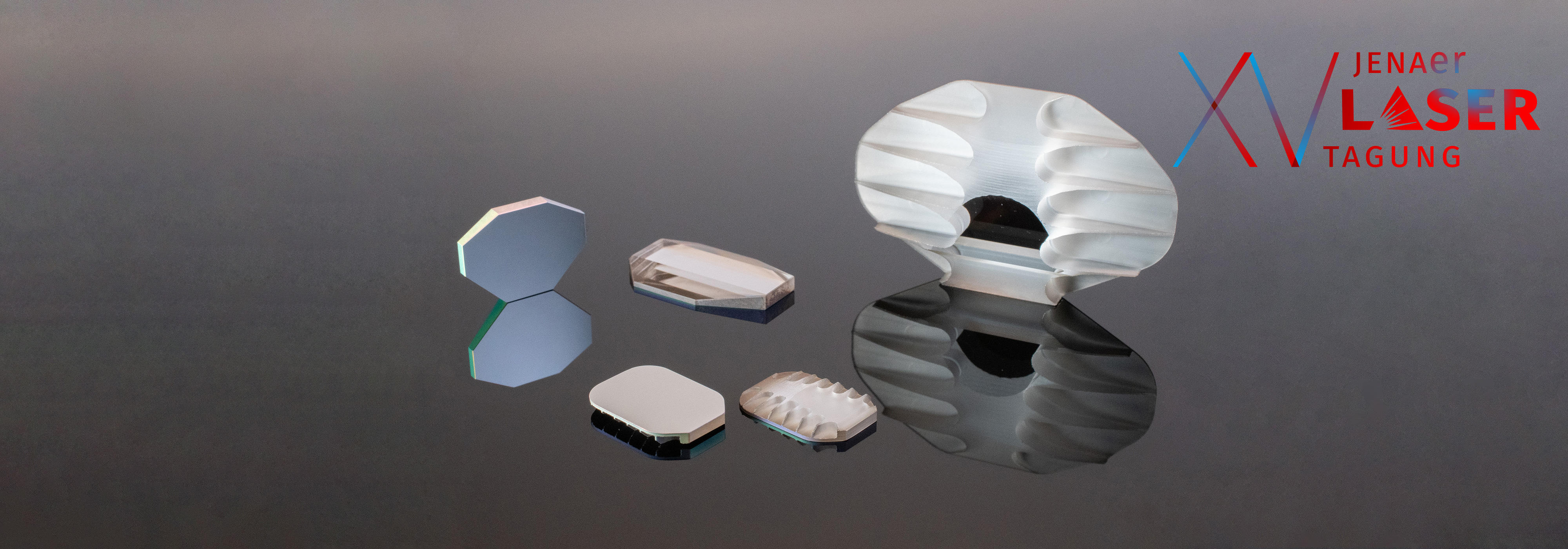
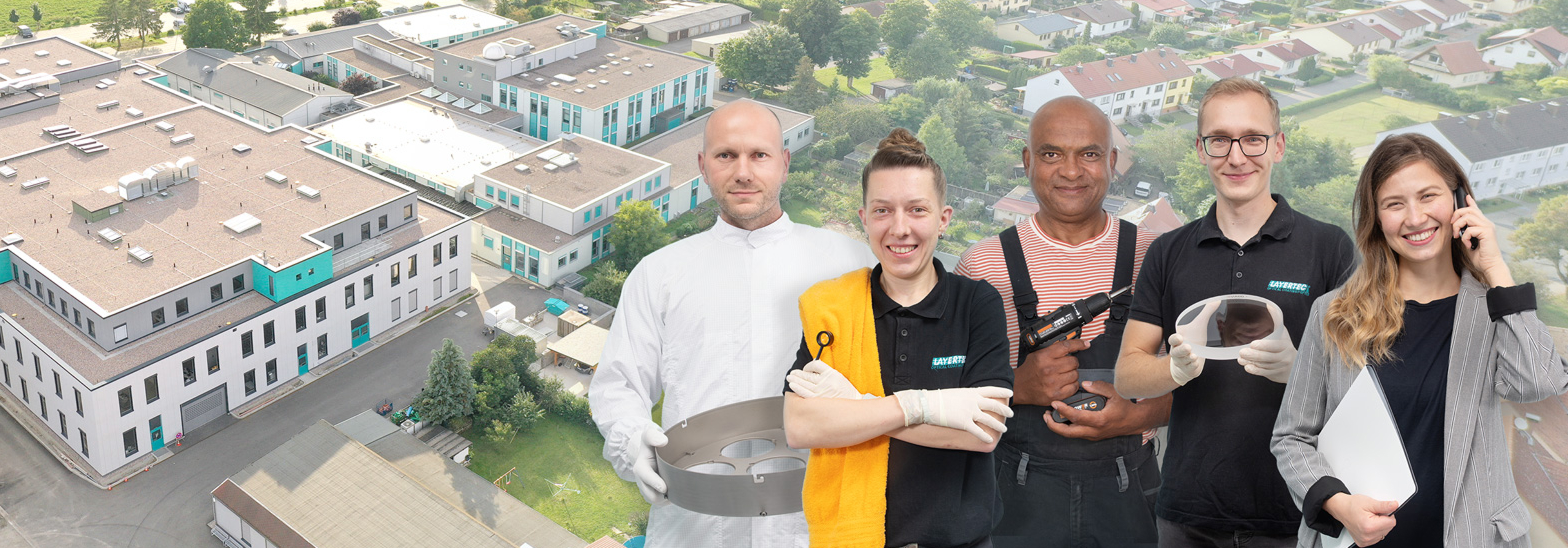
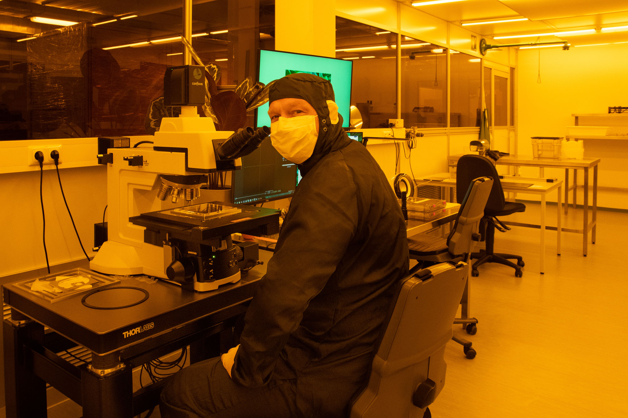
Inside the production
Industries
Processes & technical limits
| Processes | Tolerance | Max. part | Weight | Lot size | Materials |
|---|---|---|---|---|---|
| Precision optics manufacturing (grinding, polishing, cleaning of mirror substrates, lenses, prisms)Engineering | Diameter +0/-0.1 mm; thickness ±0.1 mm; surface form λ/10 · < 0.2 nm (fused silica) | 600 mm (diameter, standard fused | – | ~229,700 pieces/year | Fused silica, N-BK7, CaF2, Sapphire, YAG, ULE, Zerodur, Si |
| Magnetron sputtering (optical coatings)Surface | – | Substrates up to 60 cm diameter | – | – | Oxides, Fluorides, Metals |
| Ion beam sputtering (IBS)Surface | – | Substrates up to 30 cm diameter | – | – | Oxides, Fluorides, Metals |
| Thermal and electron beam evaporation (vacuum-based evaporation)Surface | – | cylindrical lenses up to 1.15 m length | – | – | Fluorides, Oxides |
| Ion-assisted deposition (IAD, ion sources APS pro / LION)Surface | – | – | – | – | Oxides, Fluorides |
| Zonal polishing (correction of planar surfaces, asphere manufacturing)Engineering | – | Optics up to 2000 mm edge length (since | – | – | Fused silica, ULE, Zerodur |
| Ultrasonic drilling/machining of glass substrates (e.g. conical bores)Engineering | – | – | – | – | Fused silica |
| Ultrasonic cleaning (automated, coated and uncoated substrates)Surface | – | – | – | – | Fused silica, Glass, Crystals |
| Laser engraving (on fused silica components)Surface | – | – | – | – | Fused silica |
| LithographySurface | – | – | – | – | – |
| Activation bonding/joining of surface-activated polished surfaces (laser bonding)Joining | – | – | – | – | Fused silica, Glass |
| Optical and optomechanical assembly technology (assemblies)Assembly | – | – | – | – | Fused silica, Glass, Metals |
| Solderable coatings (Solderable Coatings)Surface | – | – | – | – | – |
| Dicing/drilling of miniaturized optics from coated platesEngineering | – | – | – | – | Fused silica, Glass |
| Metrology/characterization of optical properties (CRD reflectivity/transmissivity,Testing | – | – | – | – | – |
7 Anlagen & Maschinen
| Machine | Manufacturer / model | Quantity | Working area | Year built | Site |
|---|---|---|---|---|---|
| Magnetron sputtering system | – | several | Substrates up to Ø 60 cm | – | Mellingen, Germany |
| Ion beam sputtering system (IBS) | – | – | Substrates up to Ø 30 cm | – | Mellingen, Germany |
| Vacuum evaporation system (thermal/electron beam, with IAD ion sources APS pro and LION) | Bühler Alzenau GmbH APS pro, LION (ion sources) | 7 vacuum | cylindrical lenses up to 1.15 m length | – | Mellingen, Germany |
| IAD coating system | – | several | Large optics, line-beam optics | 2010, 2012 | Mellingen, Germany |
| Inline sputtering system for large optics | – | 1 | Substrates up to ~600 mm diameter | 2007 | Mellingen, Germany |
| Ultrasonic cleaning system (automated) | – | – | Optics up to 2000 mm edge length | – | Mellingen, Germany |
| Coating chambers (total, all technologies) | – | 45 | – | – | Mellingen, Germany |
Additional services
Quality
Optical properties are characterized in-house at the ppm level: reflectivity and transmissivity by the CRD method, absorption by PCI as well as automated defect inspection according to ISO 10110; in addition, GDD measuring stations are used for dispersive mirrors.
| Evidence | Mellingen |
|---|---|
| NAThüringen (Sustainability Agreement Thuringia) | |
| berufundfamilie | |
| ISO 9001 | |
| EN 9100 |
History
- 1990
Founding of LAYERTEC (optical coatings) GmbH by Hartmut Heyer as the first spin-off of Friedrich Schiller University Jena after reunification
- 1992
Start of production of magnetron-sputtered coating systems
- 1993
Establishment of an in-house substrate production with precision opticians from the former VEB Carl Zeiss Jena
- 1994
Complete production chain from raw glass available
- 1995
First sale of evaporated fluoride/oxide systems for UV applications
- 1997
Expansion of the classic production chain, miniaturization and first dispersive mirrors for customers from Vienna
- 1998
Set-up of an online shop
- 2002
Move to the current location in Mellingen
- 2007
First IBS coating machines and inline sputtering system for substrates up to approx. 600 mm
- 2010–2012
Expansion of the production area through new buildings, installation of modern IAD systems; from approx. 2012 in-house asphere manufacturing
- 2013
Conversion of production control to SAP
- 2015
Laser marking of all finished fused silica components
- 2017
Manufacturing of optics with 2000 mm edge length; investments in joining/bonding technologies
- 2018
Ultrasonic technologies for new glass geometries; participation in NAThüringen since 1.10.2018
- 2020
Over 30 years on the market
- 2025
Renewal of the NAThüringen certification on 5.9.2025 on the occasion of the 35th company anniversary