
LayTec develops and manufactures integrated in-situ and in-line metrology for thin-film processes in semiconductor and photovoltaic manufacturing.
LayTec AG
Berlin (Headquarter) · Berlin (Application and Support / Service)New on Amplifa
About LayTec
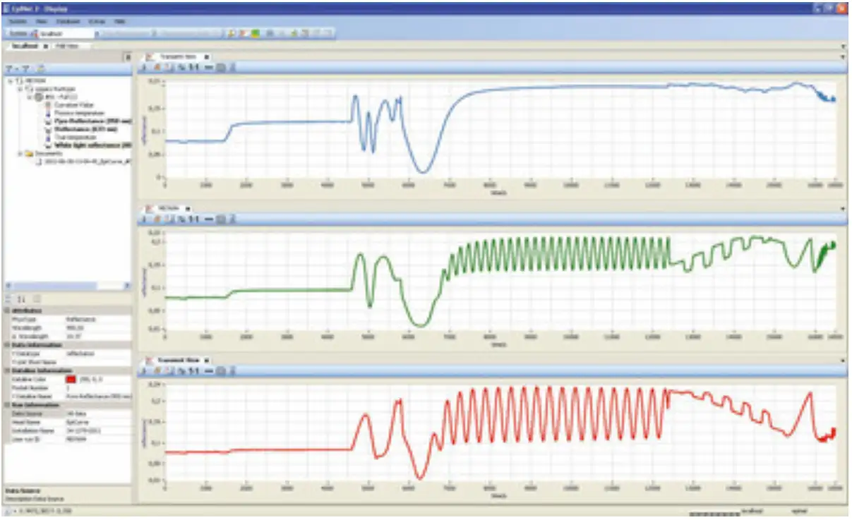
LayTec AG develops and produces metrology-based measurement systems for process control in the semiconductor and photovoltaic industries. The portfolio includes in-situ, in-line, lab-line and map-line metrology for real-time monitoring of deposition processes: layer thickness, band gap, reflectance, transmittance, sheet resistance, temperature, wafer curvature and charge carrier lifetime are measured contactlessly during the process. Products include InspiRe (spectral in-situ monitoring for spin coating, slot-die coating, PVD and annealing processes), Flames and ILMetro (in-line monitoring of large-area multilayer structures), PearL/t-PearL (photoluminescence), EpiTT and EpiCurve TT (temperature and curvature measurement for 2D materials), TRIton (end-point metrology for plasma etching) and the C2C mapping station EpiX. Application fields are compound semiconductors, Si thin-film characterization, perovskite and organic photovoltaics, CIGS, 2D materials such as graphene, hBN and WS2, as well as displays and large-area coating. More than 3500 systems are installed worldwide. LayTec manufactures in Berlin and supports customers through a global sales and service network under DIN EN ISO 9001:2015.
- Site
- Berlin
- Processes
- In-situ metrology for deposition processes – real-time process control, In-line metrology during substrate transfer between depositions, In-situ monitoring of thin-film formation during spin coating, slot-die coating, PVD and, In-line monitoring of multilayer thin-film structures in large-area processes (spectral, In-situ/in-line photoluminescence (PL), time-dependent PL for charge carrier lifetime measurement, In-situ monitoring of epitaxial deposition of 2D materials (reflectance, deflection,, End-point metrology for plasma etch processes (TRIton), Optical inspection in thin-film production lines: layer thickness, reflectance, transmittance,
- Materials
- Perovskite (perovskite-based solar cells), Silicon (Si-perovskite tandem), Graphene, Hexagonal boron nitride, Tungsten disulfide, CIGS (copper indium gallium selenide), III-V compound semiconductors, Organic PV materials
- Certificates
- DIN EN ISO 9001:2015, ISO 9001
- Founded
- 1999
- Industries
- Semiconductor industry (compound semiconductor, Si thin film), Photovoltaics (perovskite, organic PV, CIGS, Si tandem), Large-Area Coating / Display, 2D materials, Research institutions, OEM customers
- 01
Engineering (optics, electronics, software, physics)
- 02
Manufacturing of the measurement systems
- 03
Installation and commissioning at the customer
- 04
Application support and training
- 05
Service, calibration and maintenance
- 06
Data analysis and process optimization
Measurement Methods and Applications
Perovskite (perovskite solar cells)
In-situ and in-line monitoring of film formation during spin coating, slot-die coating, PVD and annealing processes.
Silicon (Si-perovskite tandem)
Optical inspection of thin-film parameters in perovskite solar glass production lines.
Organic PV and hybrid materials
Measurement of layer thickness, band gap and sheet resistance in R2R and S2S configurations.
CIGS (copper indium gallium selenide)
Spectral reflectance measurement for monitoring thin-film deposition.
2D materials (graphene, hBN, WS2)
In-situ monitoring of epitaxial CVD deposition using reflectance, deflection and emissivity-corrected pyrometry.
III-V compound semiconductors
In-situ metrology for LED and LASER epitaxy (in-situ market leader according to company history).
Locations

Berlin – Headquarter
DEHeadquarters, development and manufacturing
- Materials
- Measurement systems for semiconductor and PV thin-film processes
- InspiRe
- Flames
- ILMetro
- PearL / t-PearL
- EpiTT
- EpiCurve TT
- TRIton
- EpiX

Berlin – Application and Support
DEApplication and Support / Service with 24h response time (WERKtage CET)
Metrology Systems
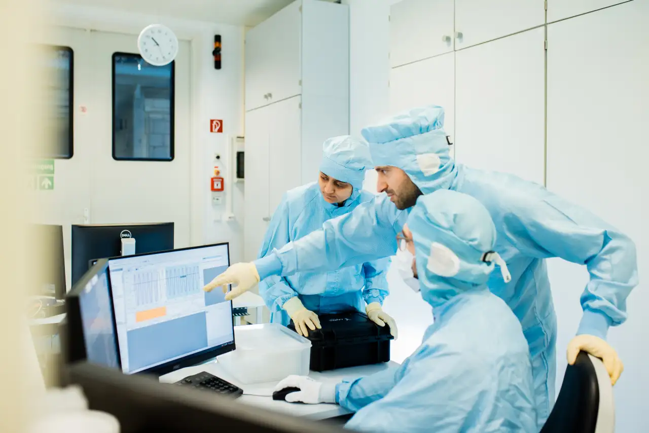
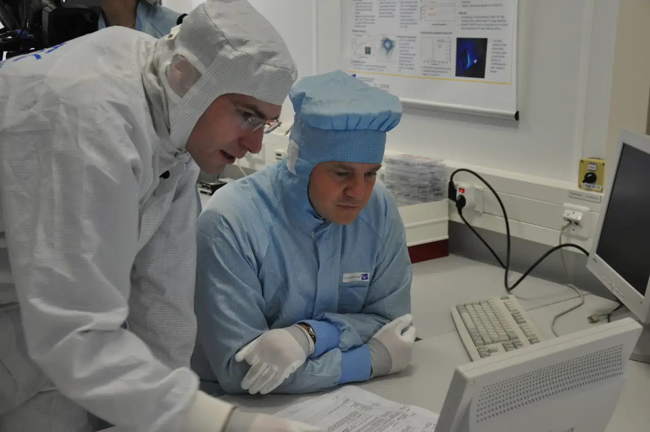
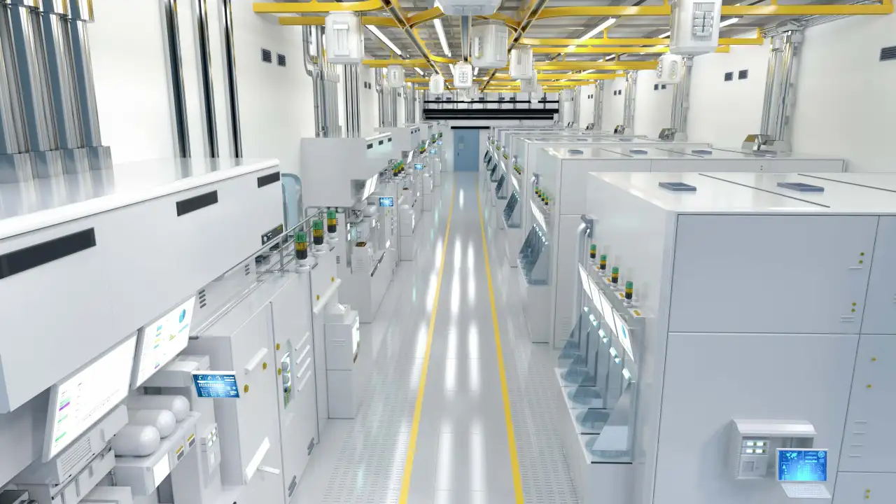
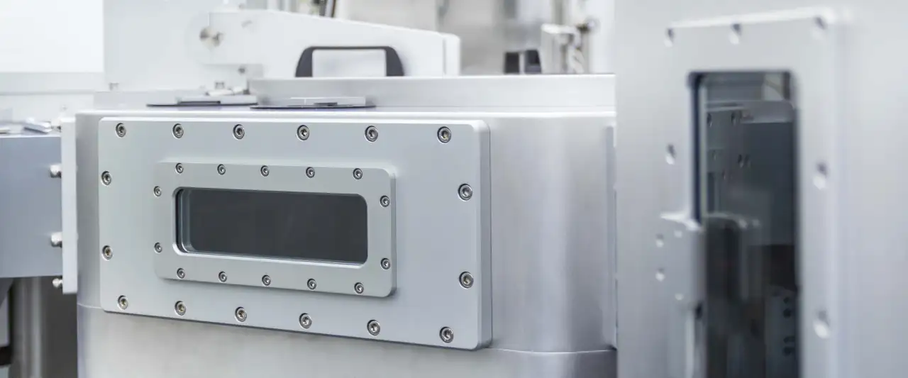
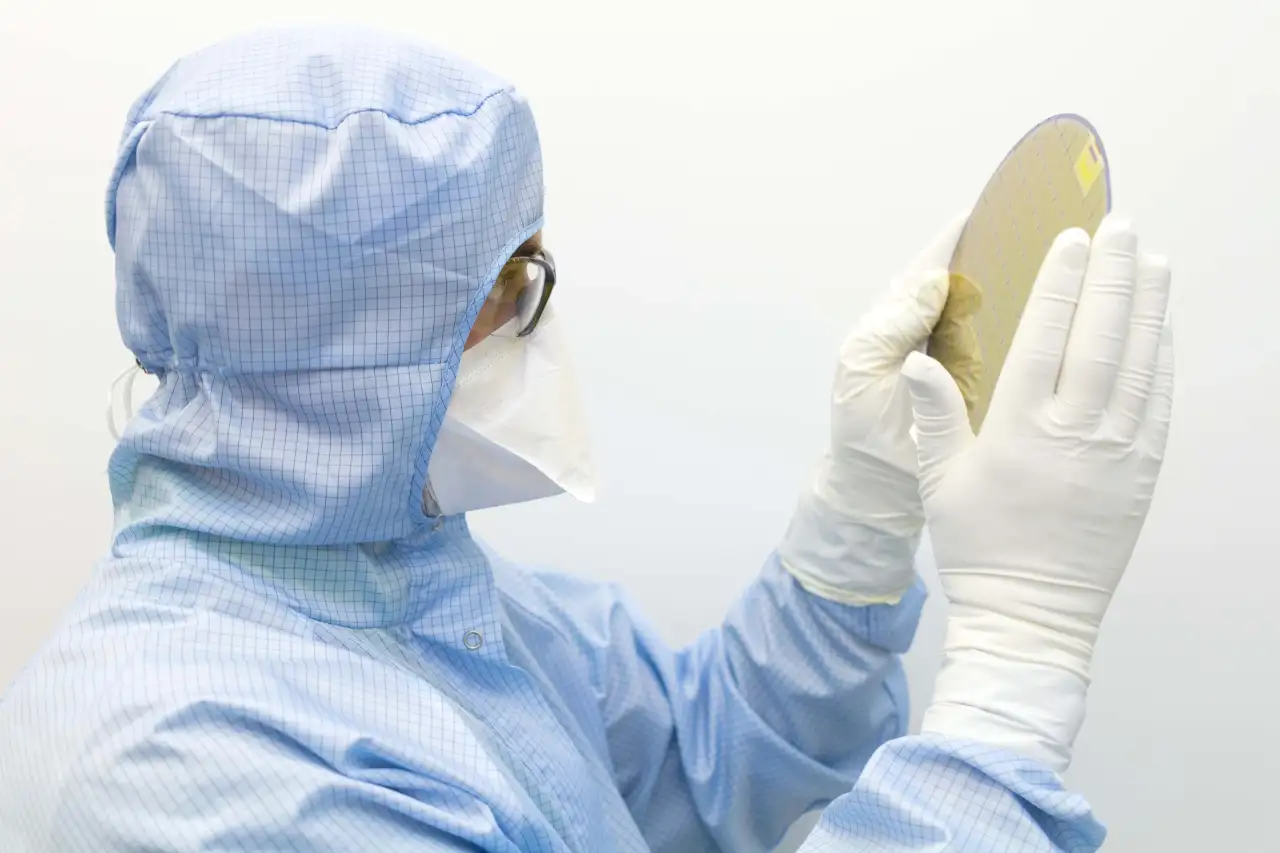
Inside the production
Industries
Processes & technical limits
| Processes | Tolerance | Max. part | Weight | Lot size | Materials |
|---|---|---|---|---|---|
| In-situ metrology for deposition processes – real-time process controlTesting | – | – | – | – | perovskite, organic PV materials, hybrid materials, graphene, hexagonal boron nitride (hBN), tungsten disulfide (WS2), III-V compound semiconductors, CIGS, silicon thin film |
| In-line metrology during substrate transfer between depositionsTesting | – | – | – | – | thin-film PV materials, perovskite |
| In-situ monitoring of thin-film formation during spin coating, slot-die coating, PVD andTesting | – | – | – | – | perovskite, organic PV materials, hybrid materials, CIGS |
| In-line monitoring of multilayer thin-film structures in large-area processes (spectralTesting | – | – | – | – | perovskite, thin-film PV materials |
| In-situ/in-line photoluminescence (PL), time-dependent PL for charge carrier lifetime measurementTesting | – | – | – | – | perovskite |
| In-situ monitoring of epitaxial deposition of 2D materials (reflectance, deflection,Testing | – | – | – | – | graphene, hBN, WS2, 2D materials |
| End-point metrology for plasma etch processes (TRIton)Testing | – | – | – | – | semiconductor thin films |
| Optical inspection in thin-film production lines: layer thickness, reflectance, transmittance,Testing | – | – | – | – | perovskite on glass, silicon PV thin films |
9 Anlagen & Maschinen
| Machine | Manufacturer / model | Quantity | Working area | Year built | Site |
|---|---|---|---|---|---|
| Spectral in-situ monitoring system | LayTec InspiRe | – | – | – | Berlin |
| In-line monitoring system for large-area thin-film structures | LayTec Flames | – | – | – | Berlin |
| In-line control system with multiple contactless measurements | LayTec ILMetro | – | – | – | Berlin |
| PL metrology for room-temperature deposition processes | LayTec PearL / t-PearL | – | – | – | Berlin |
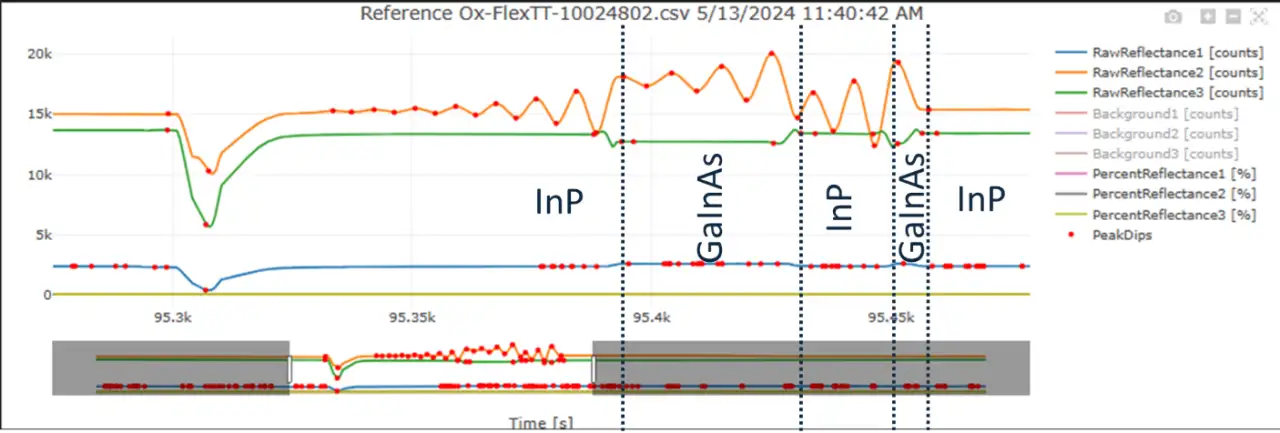
| In-situ temperature/reflectance measurement system (3 wavelengths) | LayTec EpiTT | – | – | – | Berlin |
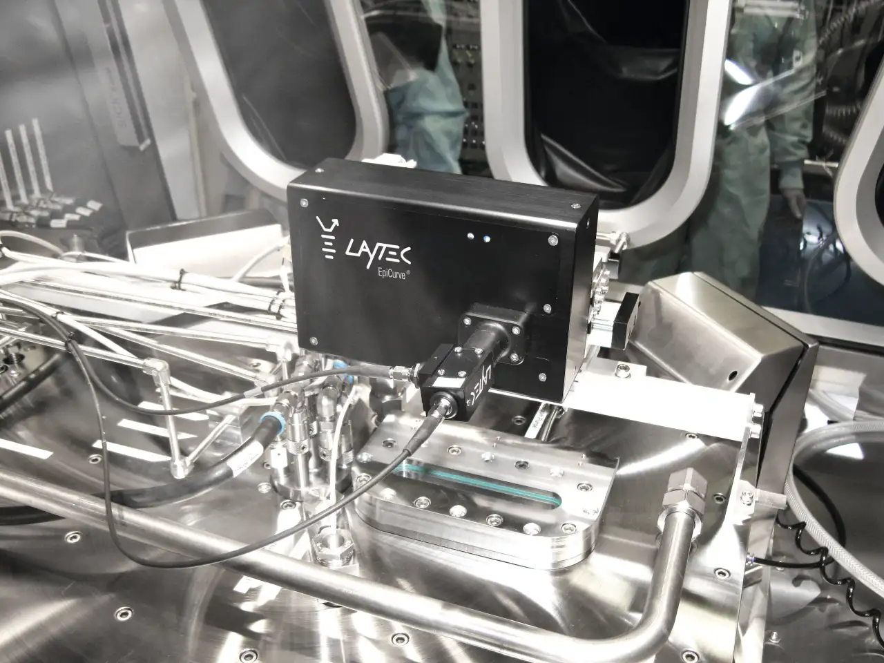
| Wafer curvature measurement system with emissivity-corrected pyrometry | LayTec EpiCurve TT | – | – | – | Berlin |
| End-point metrology system for plasma etching | LayTec TRIton | – | – | – | Berlin |
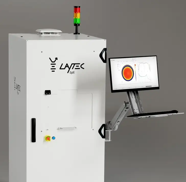
| Optical wafer characterization / C2C mapping station | LayTec EpiX | – | – | – | Berlin |
| Automated optical inspection for thin-film production lines | LayTec | – | – | – | Berlin |
Additional services
Reference customers
Quality and Certification
LayTec maintains a quality management system certified according to DIN EN ISO 9001:2015. The Application and Support team offers installation, calibration and training services as well as service contracts with 24-hour response time.
| Evidence | Berlin |
|---|---|
| ISO 9001 |
History
- 1999
Founding of LayTec GmbH; quickly became the world market leader for in-situ metrology in LED and LASER production
- 2008
Expansion into applications beyond the semiconductor industry; in-line metrology for thin-film PV and displays
- 2009–2011
Ranked among the 50 fastest-growing technology companies in Germany
- 2011
Acquisition of the assets of ORS (Optical Reference Systems), today LayTec UK
- 2018
LayTec becomes part of the Nynomic AG portfolio
- 2025
Caelux selects LayTec for optical quality inspection in perovskite solar glass production
- 2026
Sandia National Laboratories selects LayTec's EpiX for optical wafer characterization