
Design and verification services for analog, mixed-signal, and digital semiconductor ICs.

leadIC Design
New on Amplifa
About leadIC Design
leadIC Design is a provider of design and verification services for the semiconductor industry. The service portfolio includes analog and mixed-signal design including layout (AMS Design & Layout) with optimized floorplanning, device matching, and signal integrity, design verification for SoCs and IPs (SystemVerilog/UVM), physical design & verification including a Netlist-to-GDSII flow with floorplanning, timing closure, and physical verification, RTL design, DFT (Design for Testability), and FPGA design for real-time data processing, communication systems, and embedded applications. Referenced projects include the delivery of a 7-nm SmartNIC product within nine months in a complete Netlist-to-GDSII flow with 14 blocks owned by leadIC, as well as analog IP blocks (SERDES, LDO, GPIO, LVDS) in deep-submicron technology under ultra-low-power requirements. Customers are international semiconductor companies; reference projects include USB, AMBA, and PCIe verification IPs. A location is not specified on the website.
- Processes
- Analog/MS Design & Layout (AMS Design & Layout), SoC/IP Design & Verification (SoC/IP DV), Physical Design & Verification, RTL Design, DFT (Design for Test), FPGA Design, Netlist-to-GDSII Flow (Floorplanning, Timing Closure, Physical Verification), SPEC2GDS of Analog IPs (SERDES, LDO, GPIO, LVDS)
- Materials
- AMS Design & Layout, SoC/IP Design & Verification, Physical Design & Verification, RTL Design, DFT (Design for Test), FPGA Design
- Industries
- Semiconductor industry, Semiconductor Design Services
- 01
Specification and design (RTL or AMS)
- 02
Design Verification (SystemVerilog/UVM)
- 03
Physical Design (Floorplanning, Placement)
- 04
Timing Closure
- 05
Physical Verification
- 06
GDSII Delivery
Services & Processes
AMS Design & Layout
Analog and mixed-signal IC design with optimized floorplanning, device matching, and robust signal integrity.
SoC/IP Design & Verification
Validation of SoC and IP designs using SystemVerilog/UVM including integration of USB and AMBA verification IPs.
Physical Design & Verification
Netlist-to-GDSII flow with floorplanning, die-size calculation, timing closure, and physical verification.
RTL Design
Efficient and scalable hardware descriptions for high-performance digital systems.
DFT (Design for Test)
Integration of testability for improved fault detection and reduced manufacturing costs.
FPGA Design
FPGA solutions for real-time data processing, communication systems, and embedded applications.
Projects & Services

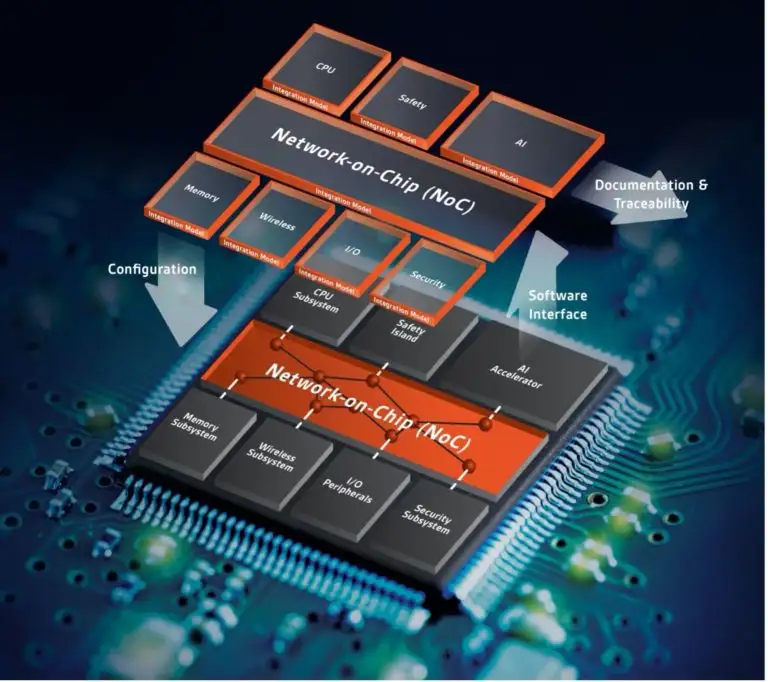




Inside the production



Industries
Processes & technical limits
| Processes | Tolerance | Max. part | Weight | Lot size | Materials |
|---|---|---|---|---|---|
| Analog/MS Design & Layout (AMS Design & Layout)Engineering | – | – | – | – | – |
| SoC/IP Design & Verification (SoC/IP DV)Engineering | – | – | – | – | – |
| Physical Design & VerificationEngineering | – | – | – | – | – |
| RTL DesignEngineering | – | – | – | – | – |
| DFT (Design for Test)Engineering | – | – | – | – | – |
| FPGA DesignEngineering | – | – | – | – | – |
| Netlist-to-GDSII Flow (Floorplanning, Timing Closure, Physical Verification)Engineering | – | – | – | – | – |
| SPEC2GDS of Analog IPs (SERDES, LDO, GPIO, LVDS)Engineering | – | – | – | – | – |
| Power Network Design (IC)Engineering | – | – | – | – | – |
Additional services
History
- 2018
Copyright notice 2018 on the website (founding year not verified)