Engineering service provider for end-to-end development of SoCs, ASICs, FPGAs as well as embedded and cloud software

LeadSOC Technologies Pvt. Ltd. / LeadSoc GmbH
Bangalore, India · Santa Clara, USA · Munich, GermanyNew on Amplifa
About LeadSOC Technologies
LeadSOC Technologies is an internationally active engineering service provider for semiconductor and embedded development headquartered in Bangalore with offices in Santa Clara (USA) and Munich. The company offers end-to-end VLSI design services across the entire development cycle: digital front-end and back-end, analog and custom design, physical design, synthesis and DFT as well as IP/SoC verification and emulation with UVM, Palladium, Zebu and FPGA environments. The chip design services are complemented by RF and hardware design including schematic entry and PCB design, post-silicon support with wafer testing and ATE, as well as DSP, embedded and platform software through to application and cloud solutions. Using AI-assisted design methods, LeadSOC covers technology nodes from 180 nm to 2 nm and, according to its own statements, works for global OEMs, ODMs and chip manufacturers in industries such as semiconductors, telecom, automotive, IoT and healthcare. At the Munich location, LeadSoc GmbH is established as the European subsidiary; the European activities are led by Veena S Chakravarthi as VP Global R&D and Head of European Operations.
- Site
- München
- Processes
- VLSI Design Services (End-to-End SoC/ASIC Design), Digital Design (IP Design, SoC Integration, Low Power Multi-Clock Design, Synthesis, STA), IP/SOC Verification & Emulation (UVM, OVM, GLS, Palladium/Zebu/FPGA Verification Environment), FPGA Design / ASIC Emulation (Synthesis, P&R, Timing Closure, Board Bring-up), Physical Design (Floorplan, CTS/STA/PV, IR/LP Checks, Tapeout), Synthesis & DFT (DCG/DCT, ATPG, MBIST, BSCAN, JTAG), Analog & Custom Design (Analog Design/Layout, Standard Cells, Memory Layout, AMS Verification), RF & Hardware Design (RF Subsystem, Board Design, Schematic Entry & PCB Design)
- Materials
- 180 nm technology node, 2 nm technology node, Technology node 180 nm, Technology node 2 nm, UVM/OVM verification, FPGA design & ASIC emulation, RF & hardware design
- Certificates
- ISO 9001, ISO 27001, TISAX, ISO 9001 (QMS aligned), ISO 27001 (ISMS aligned), TISAX (where applicable)
- Industries
- Semiconductors, Telecom, Automotive, IoT, Healthcare, Optical
- 01
Requirements analysis and design definition (requirement to GDS)
- 02
RTL design and digital IP/SoC integration
- 03
Functional verification and emulation (UVM, Palladium, Zebu, FPGA)
- 04
Synthesis, DFT and sign-off (STA, ATPG, MBIST, BSCAN, JTAG)
- 05
Physical design and tapeout
- 06
FPGA validation or ASIC emulation and board bring-up
- 07
Post-silicon support: prototyping, wafer testing, ATE
- 08
Embedded, platform and application software through to cloud solutions
Technologies & Methods
Technology node 180 nm
Older technology node, which LeadSOC serves for legacy and custom chip designs.
Technology node 2 nm
Advanced technology node for high-performance, power-efficient SoC designs.
UVM/OVM verification
Methodology for building complete verification environments for IPs and SoCs, including coverage-driven verification.
FPGA design & ASIC emulation
Retargeting of ASIC code to Xilinx, Intel, Microsemi and Lattice FPGAs for validation and system emulation.
RF & hardware design
Schematic entry, PCB design and board bring-up for RF subsystems and board designs.
Locations
Bangalore
INHeadquarters / Design Center
- VLSI Design Lab / Advanced Labs
- Embedded Software Lab with reference boards
- Emulation and verification environments (Cadence Palladium, Synopsys Zebu, FPGA)
Santa Clara
USBranch office (LeadSOC Technologies Inc.)
Munich
DEBranch office (LeadSoc GmbH)
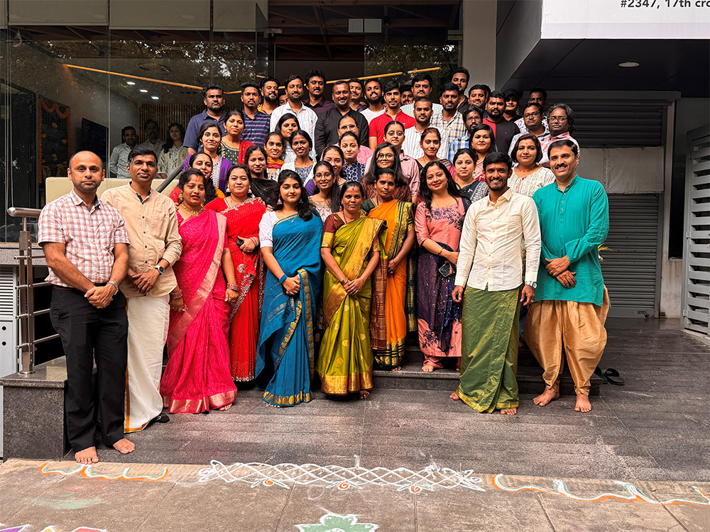
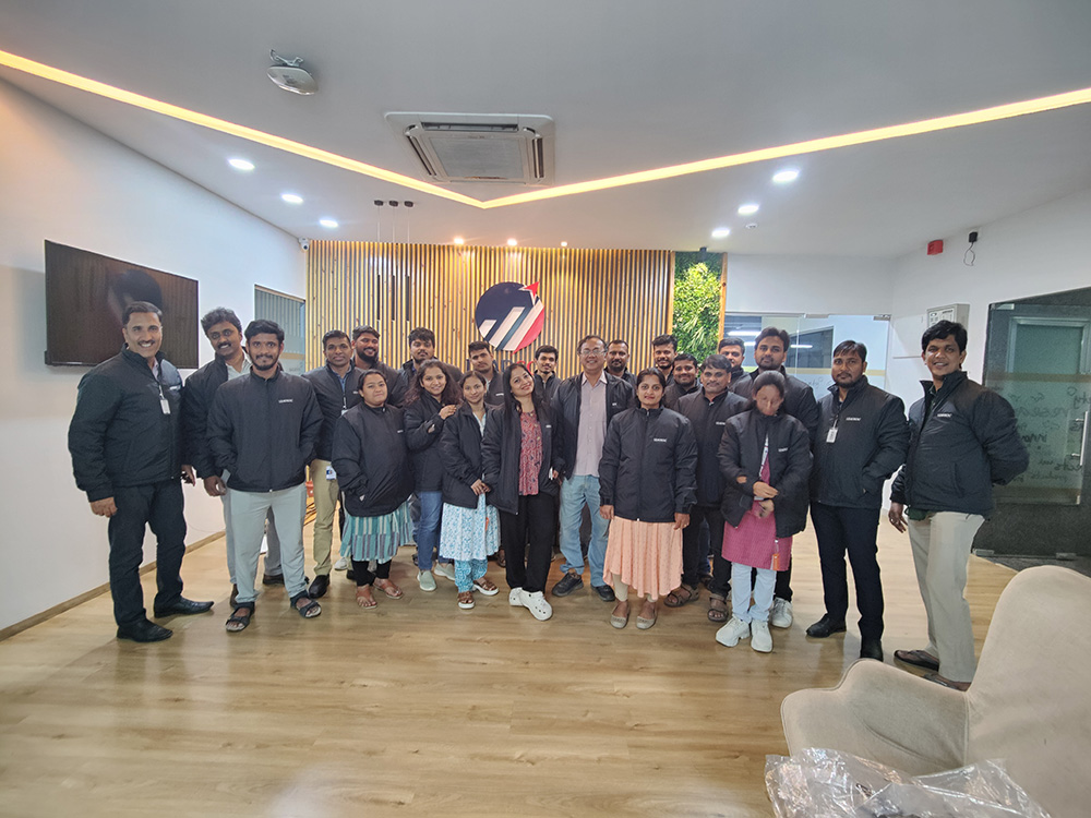
Inside the production




Industries
Processes & technical limits
| Processes | Tolerance | Max. part | Weight | Lot size | Materials |
|---|---|---|---|---|---|
| VLSI Design Services (End-to-End SoC/ASIC Design)Engineering | – | – | – | – | Silicon (semiconductor design, 180 nm to 2 nm) |
| Digital Design (IP Design, SoC Integration, Low Power Multi-Clock Design, Synthesis, STA)Engineering | – | – | – | – | – |
| IP/SOC Verification & Emulation (UVM, OVM, GLS, Palladium/Zebu/FPGA Verification Environment)Engineering | – | – | – | – | – |
| FPGA Design / ASIC Emulation (Synthesis, P&R, Timing Closure, Board Bring-up)Engineering | – | – | – | – | – |
| Physical Design (Floorplan, CTS/STA/PV, IR/LP Checks, Tapeout)Engineering | – | – | – | – | – |
| Synthesis & DFT (DCG/DCT, ATPG, MBIST, BSCAN, JTAG)Engineering | – | – | – | – | – |
| Analog & Custom Design (Analog Design/Layout, Standard Cells, Memory Layout, AMS Verification)Engineering | – | – | – | – | – |
| RF & Hardware Design (RF Subsystem, Board Design, Schematic Entry & PCB Design)Engineering | – | – | – | – | – |
| Post Silicon Support (Prototyping, Wafer Testing, Test Automation & ATE Support)Testing | – | – | – | – | – |
| DSP, Embedded & Platform Software EngineeringEngineering | – | – | – | – | – |
| Application Software & Cloud Solutions (Mobile Apps, Full-Stack, Microservices, AI/ML, Big Data)Engineering | – | – | – | – | – |
| AI Powered Design Services (AI-based RTL development, Verification, Coverage Closure, Design)Engineering | – | – | – | – | – |
| HW-SW Co-Design for processor-based systemsEngineering | – | – | – | – | – |
3 Anlagen & Maschinen
| Machine | Manufacturer / model | Quantity | Working area | Year built | Site |
|---|---|---|---|---|---|
| Hardware emulation/verification environment (Palladium, Zebu, FPGA) | Cadence (Palladium) / Synopsys (Zebu) / Xilinx, Intel, Microsemi, Lattice (FPGA) Palladium, Zebu | – | – | – | – |
| Embedded Software Lab with reference boards | – | – | – | – | – |
| VLSI Design Lab / Advanced Labs | – | – | – | – | – |
Additional services
Reference customers
Quality & Information Security
In accordance with its Quality & Information Security Policy, LeadSOC maintains a quality and information security management system aligned with ISO 9001 and ISO 27001 and, where applicable, with TISAX assessment targets. Continuous improvement is ensured through customer feedback, internal audits, corrective actions and management reviews.
| Evidence | Bangalore | Santa Clara | Munich |
|---|---|---|---|
| ISO 9001 (QMS aligned) | |||
| ISO 27001 (ISMS aligned) | |||
| TISAX (where applicable) |