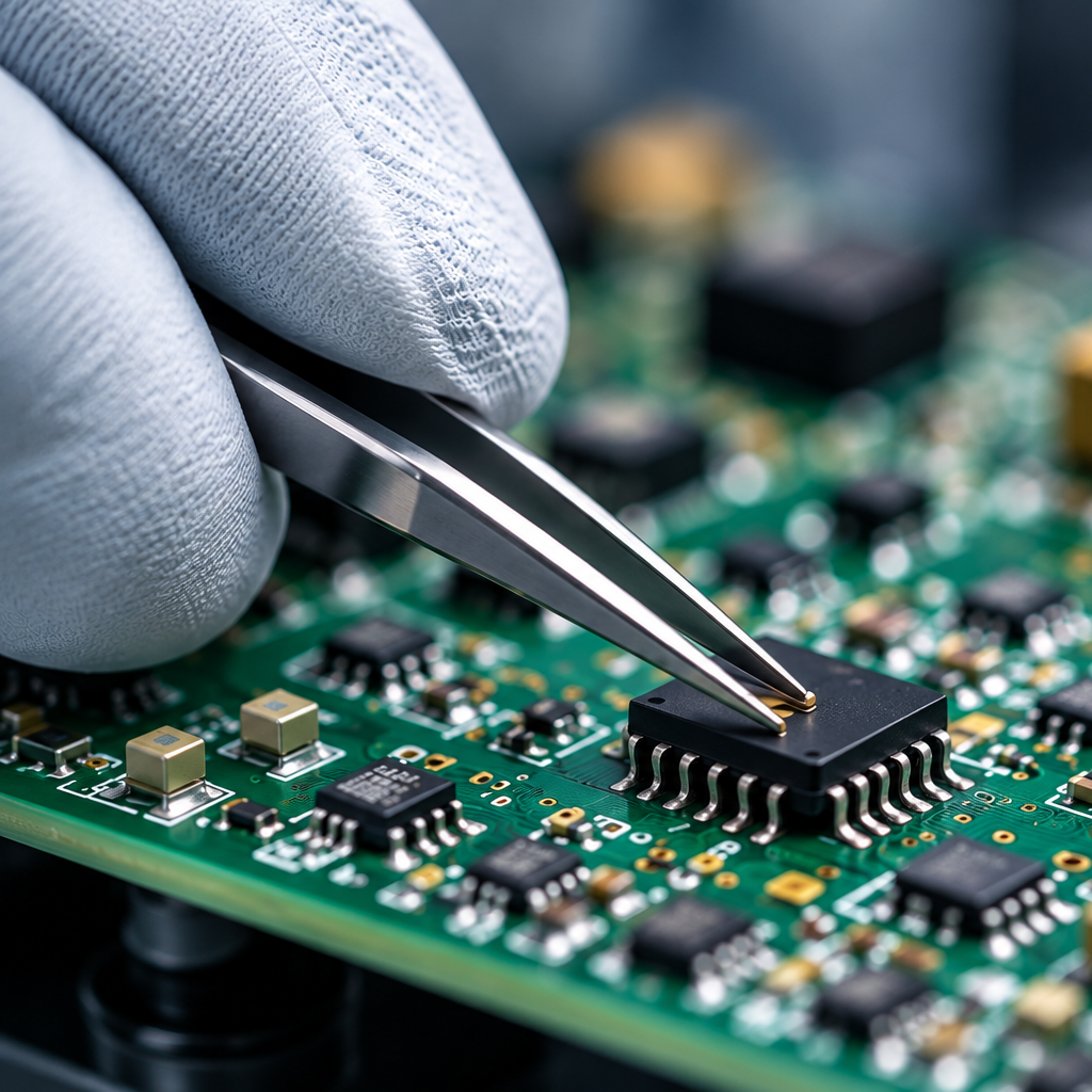
Development and manufacturing of custom electronics – from circuit design through SMD assembly to the finished device
Leder Elektronik Design GmbH
MannheimNew on Amplifa
Electronics development and manufacturing since 2001
Leder Elektronik Design GmbH develops and manufactures custom electronic solutions for industrial customers. The service portfolio includes analog and digital circuit design, PCB layout up to 16 layers including flex and microvia design, firmware development for microcontrollers in C/C++, FPGA development in VHDL, application programming in C# as well as enclosure design. In manufacturing, the company handles material sourcing and procurement planning, SMD/THT assembly, assembly of complete devices, and UV printing for finishing enclosures and components. Production runs from a quantity of 1, including prototypes, up to large series with call-off management. In addition, EMC preliminary investigations, thermal analyses, CRA, automated testing, as well as fault analysis and repair of electronic assemblies are offered. Founded in 2001 in Ketsch and operating as a GmbH since 2019, the company is based in Mannheim and serves customers from sectors such as aerospace, mechanical engineering, image processing and industrial automation.
- Site
- Mannheim
- Processes
- Analog and digital circuit design, PCB layout up to 16 layers (including flex and microvias), Microcontroller programming (C / C++), FPGA development (VHDL), Application programming (C#), Enclosure design, EMC investigations / EMC preliminary investigation, Thermal analysis
- Materials
- PCBs up to 16 layers, UV printing
- Certificates
- Automated testing, EMC preliminary investigation / Pre-Compliance, ISO 9001
- Founded
- 2001
- Industries
- Aerospace, Mechanical and plant engineering, Image processing, Industrial automation, IT and software
- 01
Circuit and PCB design
- 02
Firmware/FPGA/software development
- 03
Enclosure design
- 04
Material sourcing and procurement planning
- 05
SMD/THT assembly
- 06
Assembly of complete devices
- 07
Automated testing
- 08
Repair service and product support
Development and manufacturing processes
PCBs up to 16 layers
Multilayer PCBs including flex and microvia design for custom electronics.
UV printing
Direct labeling and finishing of enclosures and components.
Location
Mannheim
DECompany headquarters with development, manufacturing and service
- Lot size
- Quantity 1 to large series
- Materials
- PCBs up to 16 layers, flex, microvias
- SMD/THT assembly
- UV printing
- Automated testing
Services and assemblies
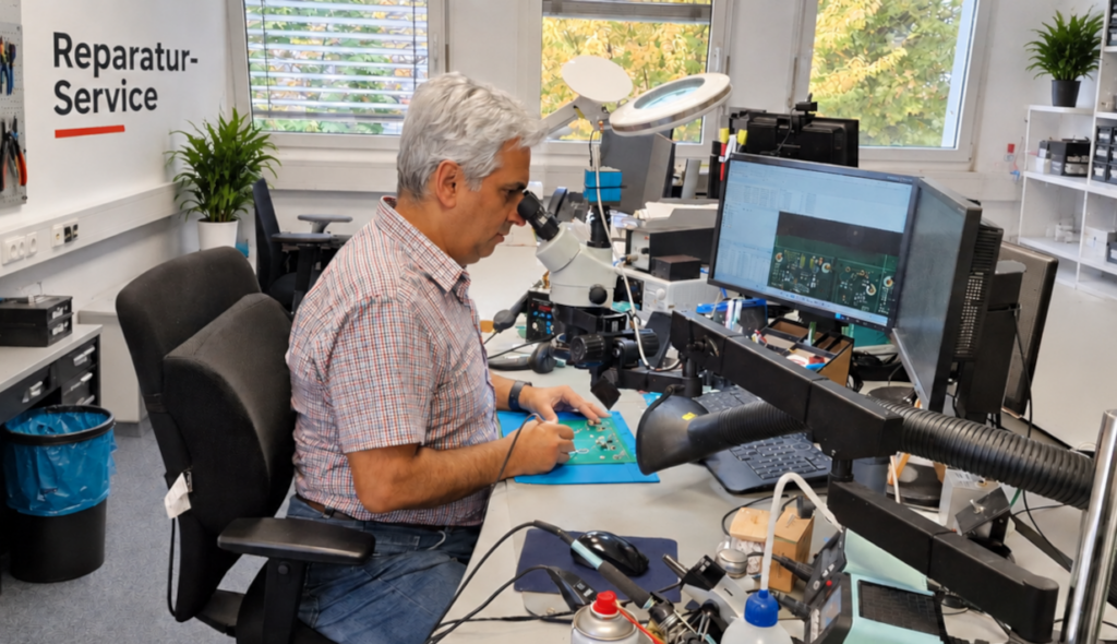
Inside the production


Industries
Processes & technical limits
| Processes | Tolerance | Max. part | Weight | Lot size | Materials |
|---|---|---|---|---|---|
| Analog and digital circuit designEngineering | – | – | – | – | – |
| PCB layout up to 16 layers (including flex and microvias)Engineering | – | – | – | – | – |
| Microcontroller programming (C / C++)Engineering | – | – | – | – | – |
| FPGA development (VHDL)Engineering | – | – | – | – | – |
| Application programming (C#)Engineering | – | – | – | – | – |
| Enclosure designEngineering | – | – | – | – | – |
| EMC investigations / EMC preliminary investigationTesting | – | – | – | – | – |
| Thermal analysisTesting | – | – | – | – | – |
| CRATesting | – | – | – | – | – |
| Material sourcing and procurement planningAssembly | – | – | – | 1 | – |
| Manufacturing from a quantity of 1 to series productionAssembly | – | – | – | 1 | – |
| SMD assembly (SMD/THT assembly)Assembly | – | – | – | – | – |
| Large series with call-off managementAssembly | – | – | – | – | – |
| Assembly of complete devicesAssembly | – | – | – | – | – |
| Automated testingTesting | – | – | – | – | – |
| Fault analysis and repair of electronic assemblies (repair service)Testing | – | – | – | – | – |
| Enclosure finishing / UV printing (direct labeling and finishing of enclosures and components)Surface treatment | – | – | – | – | – |
Additional services
Reference customers
Quality and testing
Automated testing and EMC preliminary investigations ensure the quality of manufactured assemblies. A repair service with fault analysis supports the products beyond manufacturing.
| Evidence | Mannheim |
|---|---|
| Automated testing | |
| EMC preliminary investigation / Pre-Compliance | |
| ISO 9001 |
Our history
- 2001
Founded as a sole proprietorship by Günther Leder in Ketsch, initially as a part-time business
- 2019
Conversion into a GmbH; Günther Leder takes over management on a full-time basis
- 2019
Relocation of company headquarters to Mannheim (new business premises)