Contract manufacturer for analog, mixed-signal and specialized semiconductor technologies on 200-mm silicon wafers

LFoundry S.r.l.
Avezzano (IT) · Landshut (DE)New on Amplifa
About LFoundry
LFoundry S.r.l. is a custom semiconductor manufacturer (foundry) with company headquarters and production in Avezzano, Italy. The company produces integrated circuits and specialized devices on 200-mm silicon wafers using its own technologies for 150-nm and 110-nm nodes as well as optimized CMOS image sensor (CIS) processes down to 90 nm, including back-side illumination (BSI). This is complemented by optoelectronics such as SiPM, SPAD and X-ray detectors, smart-power processes (LDMOS), MEMS, wafer thinning and stacking, DBI bonding (3D stacking), lithographic stitching, and back-end services such as wafer testing and prototype packaging. With MPW and MLM services, PDKs, IP portfolios and reference flows, LFoundry supports customers from development to volume production. Target industries include automotive, industrial, medical technology, security, science, space imaging and telecommunications. The Avezzano plant achieves a capacity of 40,000 wafers per month; sales, marketing and R&D are located in Landshut, Germany.
- Site
- Avezzano (AQ)
- Processes
- CMOS semiconductor manufacturing 150 nm (base process 1.8V MOS, 3.3V/5V options, up to 6 Al metal, CMOS semiconductor manufacturing 110 nm (1.2V core, 4-6 metal layers, lithography down to 193nm ArF), CMOS image sensor (CIS) manufacturing with optimized processes down to 90nm, Back-side illumination (BSI) technology, Optoelectronics manufacturing (SiPM, SPAD, X-ray detectors), Smart power manufacturing (LDMOS), MEMS manufacturing, Back-end services: wafer testing
- Materials
- Silicon (200mm wafer), Silicon (200-mm wafers), 150 nm CMOS technology, 110 nm CMOS technology, CMOS Image Sensor (CIS/BSI) down to 90 nm, Smart Power / LDMOS, MEMS manufacturing, Al and Cu metallization
- Certificates
- ISO 9001:2015, IATF 16949:2016, TL9000, OHSAS 18001, ISO 14001, ISO 9001:2015 (DEKRA), IATF 16949:2016 (DEKRA)
- Founded
- 2008
- Employees
- 1300+
- Industries
- Automotive, Industrial, Medical Technology, Security, Science, Space Imaging
- 01
Design Enablement (PDK, IP, Reference Flows)
- 02
MPW/MLM Service
- 03
Wafer manufacturing (CMOS 150/110 nm, CIS down to 90 nm)
- 04
Specialty modules (BSI, thinning, stacking, DBI bonding)
- 05
Back-end services (wafer testing, prototype packaging)
- 06
Delivery to customers worldwide
Technologies & Processes
Silicon (200-mm wafers)
Base material of the entire CMOS and sensor specialty manufacturing.
150 nm CMOS technology
1.8 V MOS base process with 3.3 V/5 V options, up to 6 aluminum metal layers and LDMOS up to 200 V for mixed-signal, RF and high voltage.
110 nm CMOS technology
1.2 V core process with 4–6 metal layers, lithography down to 193 nm ArF, for high-performance analog and digital products.
CMOS Image Sensor (CIS/BSI) down to 90 nm
Optimized processes including back-side illumination for image sensors, among other things in automotive and industrial applications.
Smart Power / LDMOS
High-voltage power processes up to 200 V for automotive and industrial applications.
MEMS manufacturing
Micro-mechanical devices based on standard and specialty CMOS processes.
Al and Cu metallization
Aluminum standard metallization with copper back-end-of-line for volume production at 90 nm.
Locations
Avezzano
ITCompany headquarters and manufacturing (200-mm fab)
- Lot size
- MPW/MLM up to volume production; capacity of 40,000 wafers/month
- Materials
- Silicon; CMOS 150/110 nm, CIS down to 90 nm, LDMOS, MEMS
- 200-mm semiconductor fab
- 193-nm ArF lithography
- Cleanroom manufacturing
- Wafer testing (back-end)
Landshut
DESales, marketing and R&D
Manufacturing Services

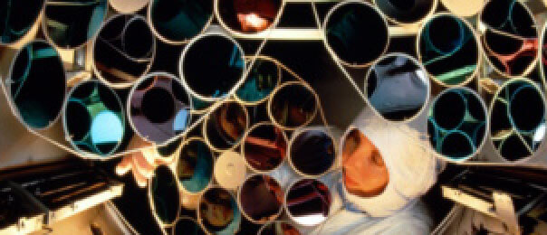
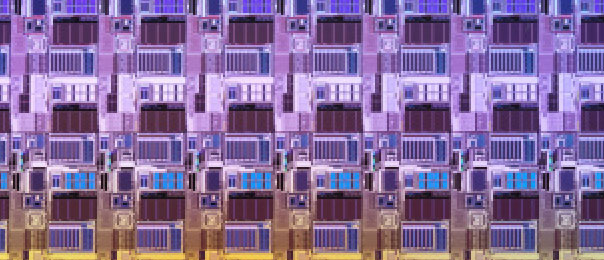
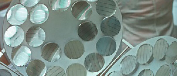
Inside the production
Industries
Processes & technical limits
| Processes | Tolerance | Max. part | Weight | Lot size | Materials |
|---|---|---|---|---|---|
| CMOS semiconductor manufacturing 150 nm (base process 1.8V MOS, 3.3V/5V options, up to 6 Al metalAdditive | – | 200 mm wafer | – | 40,000 wafers/month (total capacity) | Silicon |
| CMOS semiconductor manufacturing 110 nm (1.2V core, 4-6 metal layers, lithography down to 193nm ArF)Additive | – | 200 mm wafer | – | – | Silicon |
| CMOS image sensor (CIS) manufacturing with optimized processes down to 90nmAdditive | – | 200 mm wafer | – | – | Silicon |
| Back-side illumination (BSI) technologyAdditive | – | 200 mm wafer | – | – | Silicon |
| Optoelectronics manufacturing (SiPM, SPAD, X-ray detectors)Additive | – | – | – | – | Silicon |
| Smart power manufacturing (LDMOS)Additive | – | – | – | – | Silicon |
| MEMS manufacturingAdditive | – | – | – | – | Silicon |
| Back-end services: wafer testingTesting | – | 200 mm wafer | – | – | Silicon |
| Back-end services: prototype packagingJoining | – | – | – | – | Silicon |
| DBI bonding (3D stacking)Joining | – | 200 mm wafer | – | – | Silicon |
| Wafer thinningSurface | – | 200 mm wafer | – | – | Silicon |
| Design enablement / design services (PDK, IP portfolio, reference flows)Engineering | – | – | – | – | – |
| MPW (multi-project wafer) and MLM servicesAdditive | – | – | – | – | – |
2 Anlagen & Maschinen
| Machine | Manufacturer / model | Quantity | Working area | Year built | Site |
|---|---|---|---|---|---|
| Semiconductor fab (200mm manufacturing plant) | – | 1 | 200mm wafer | – | Avezzano, Italy |
| 193nm ArF lithography | – | – | – | – | Avezzano, Italy |
Additional services
Quality Management
The quality management system in accordance with ISO 9001:2015 and IATF 16949:2016 (DEKRA) covers the manufacturing of integrated circuits. Production environment, process control (SPC, FDC, APC) and supplier management are fully automated and follow APQP principles.
| Evidence | Avezzano |
|---|---|
| ISO 9001:2015 (DEKRA) | |
| IATF 16949:2016 (DEKRA) | |
| ISO 14001 | |
| OHSAS 18001 | |
| TL9000 |
History
- 1992
Fab in Landshut built by Hitachi (Renesas predecessor)
- 2008
Founding of LFoundry in Landshut, Germany
- 2010
Acquisition of the Landshut plant from Renesas for €1; purchase of the factory in Rousset (France) from Atmel
- 2011
Insolvency and closure of the Landshut plant (October 6, 2011)
- 2013
Insolvency of LFoundry Rousset SAS; Micron acquires the Avezzano plant
- 2014
New corporate structure in Avezzano, Italy
- 2016
SMIC acquires 70% of LFoundry S.r.l. in Avezzano
- 2017
SMIC awards the Avezzano site the 'A1 Outstanding Contribution Fab' prize
- 2018
Co-founding of the Hubruzzo Foundation (February 5, 2018)
- 2019
100% acquisition by Wuxi Xichanweixin Semiconductor for USD 112.8 million