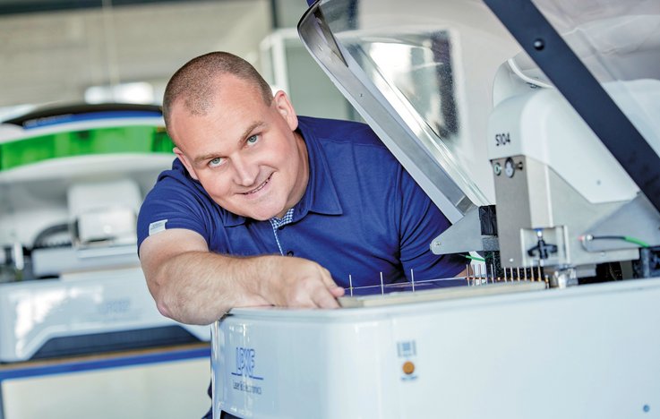
Develops and manufactures laser-based production systems for electronics, semiconductor packaging, plastic welding and solar cell structuring
LPKF Laser & Electronics SE
Garbsen · Fürth · Suhl · Naklo (SI) · Tualatin (US) · Shanghai/Suzhou/Tianjin/Shenzhen (CN) · Seoul (KR) · Bac Ninh (VN)New on Amplifa
About LPKF
LPKF Laser & Electronics SE is an internationally operating technology group headquartered in Garbsen near Hanover that develops and manufactures laser-based production solutions for demanding industries. The portfolio includes systems for Advanced Semiconductor Packaging (LIDE glass processing, Tensor Ablation/Bonding), laser depaneling of printed circuit boards, SMT Stencil Laser, laser plastic welding, Laser Transfer Printing, laser scribing for thin-film solar cells as well as systems for rapid in-house PCB prototyping and micro material processing. Materials processed include thin glass and glass substrates, FR4, LCP, ceramic (Al2O3), LTCC, copper and Epoxy Mold Compound. In addition to equipment sales, LPKF offers production services as contract manufacturing through Vitrion and LaserMicronics. The company is present in more than 60 countries and employs around 700 staff worldwide; the stock is listed in the SDAX of Deutsche Börse.
- Site
- Garbsen
- Processes
- Laser depaneling (PCB laser depaneling, CleanCut/Tensor technology), SMT Stencil Laser (manufacture of SMD stencils, step stencils, wafer stencils)., IC Packaging: Through Mold Vias (TMV), cutting and singulation of IC packages, Through Glass Vias, Laser drilling and cutting for PCB shops (rigid PCBs, FPCB, coverlayer), Laser plastic welding, Laser Transfer Printing (LTP), Laser scribing (thin-film solar cell structuring), LIDE technology (Laser Induced Deep Etching) – high-precision processing of glass/glass substrates
- Materials
- FR4, LCP (Liquid Crystal Polymer), Glass / thin glass / glass substrates, Ceramic (Al2O3), LTCC, Copper, Plastic, Epoxy Mold Compound (EMC)
- Certificates
- ISO 9001:2015, ISO 14001:2015, ISO 45001:2023, ISO 9001, ISO 14001, ISO 45001
- Founded
- 1976
- Employees
- approx. 700 worldwid
- Industries
- Semiconductors/Advanced Packaging, Electronics Manufacturing/EMS, PCB Prototyping/Research, Plastics Processing, Photovoltaics/Solar, Automotive Industry
- 01
Process development (R&D)
- 02
System development and engineering
- 03
Manufacturing and assembly of the laser systems
- 04
Sales via own subsidiaries and distributors
- 05
Commissioning, training, maintenance and upgrades
- 06
Production services (Vitrion Glass Processing Foundry, LaserMicronics)
Materials & Processes
Glass / thin glass / glass substrates
High-precision, defect-free processing via Laser Induced Deep Etching for advanced packaging and microsystems technology.
FR4
Standard material for PCB prototyping, laser drilling and structuring.
LCP (Liquid Crystal Polymer)
Substrate for picosecond-based structuring without carbonization.
Ceramic (Al2O3)
Structuring of metal layers on ceramic carriers, scribing and drilling.
LTCC
Structuring, cutting and drilling of Low-Temperature Co-fired Ceramics.
Copper
Processing of copper layers, among other things in thin-film ablation.
Epoxy Mold Compound (EMC)
Laser processing of molded IC packages, among other things Through Mold Vias.
Plastics (laser plastic welding)
Laser beam welding of plastic components for consumer electronics, medical technology and automotive.
Locations
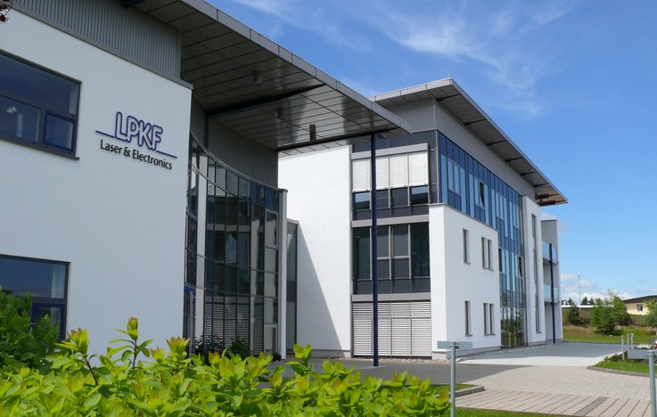
Garbsen
DEHeadquarters: development, manufacturing, sales, service; production services micro material processing.
- Materials
- Glass, thin glass, plastic, FR4, ceramic, LTCC, copper
- PicoLine picosecond laser systems
- NEXAR glass processing systems
- StencilLaser
- CuttingMaster
- ProtoMat milling drilling plotters
- ProtoLaser U4/S4/R4/H4
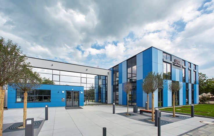
Fürth
DELPKF WeldingQuipment GmbH – systems for laser plastic welding
- Materials
- Plastic
- Laser plastic welding systems
Suhl
DELPKF SolarQuipment GmbH – system development and manufacturing for solar cell structuring
- Materials
- Thin-film solar cells
- Laser systems for solar cell structuring
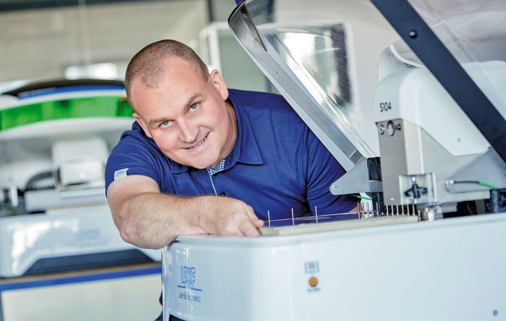
Naklo
SILPKF Laser & Electronics d.o.o. – production of prototyping equipment (sites Kranj and Naklo)
Inside the production
Industries
Processes & technical limits
| Processes | Tolerance | Max. part | Weight | Lot size | Materials |
|---|---|---|---|---|---|
| Laser depaneling (PCB laser depaneling, CleanCut/Tensor technology)Machining | – | – | – | – | rigid printed circuit boards, flexible printed circuit boards (FPCB), Coverlay |
| SMT Stencil Laser (manufacture of SMD stencils, step stencils, wafer stencils).Machining | – | – | – | – | Steel (stencils) |
| IC Packaging: Through Mold Vias (TMV), cutting and singulation of IC packages, Through Glass ViasMachining | – | – | – | – | Epoxy Mold Compound (EMC), Glass |
| Laser drilling and cutting for PCB shops (rigid PCBs, FPCB, coverlayer)Machining | – | – | – | – | FR4, Flexible printed circuit boards, Coverlay |
| Laser plastic weldingJoining | – | – | – | – | Plastic |
| Laser Transfer Printing (LTP)Surface | – | – | – | – | – |
| Laser scribing (thin-film solar cell structuring)Machining | – | – | – | – | Thin-film solar cells |
| LIDE technology (Laser Induced Deep Etching) – high-precision processing of glass/glass substratesMachining | – | – | – | – | Glass |
| Picosecond laser processing (PicoLine): structuring with 30 µm line-to-space, carbon-freeMachining | 30 µm line-to-space | – | – | – | LCP |
| Vitrion® Glass Processing Foundry Services (production services precision processing of glass)Machining | – | – | – | – | Glass, Thin glass |
| LaserMicronics® Microprocessing (production services micro material processing)Machining | – | – | – | – | – |
| Tensor AblationMachining | – | – | – | – | Glass |
| Tensor BondingJoining | – | – | – | – | Glass |
| PCB structuring (structuring printed circuit boards, mechanically and by laser)Machining | – | – | – | – | FR4 |
| PCB drilling (through holes and blind holes)Machining | – | – | – | – | FR4 |
| Through-hole plating processes (chemical-free and electroplating)Surface | – | – | – | – | – |
| Multilayer PCB manufacturing (up to eight layers)Assembly | – | – | – | – | FR4 |
| Micro material processing: cold ablation of thin films with picosecond lasers (e.g. OLED,Machining | Cutting kerfs down to 15 µm | – | – | – | FR4, Ceramic (Al2O3), LTCC, Copper, Glass |
| Structuring of metal layers on ceramic carriers, ceramic scribing, LTCCMachining | – | – | – | – | Ceramic (Al2O3), LTCC |
| Active Mold Packaging (AMP)Machining | – | – | – | – | – |
| MicroVia drillingMachining | – | – | – | – | – |
14 Anlagen & Maschinen
| Machine | Manufacturer / model | Quantity | Working area | Year built | Site |
|---|---|---|---|---|---|
| Picosecond laser system (PicoLine) | LPKF PicoLine | – | – | – | – |
| Laser depaneling system (CuttingMaster) | LPKF CuttingMaster | – | – | – | – |
| PCB milling drilling plotter | LPKF ProtoMat S104 | – | – | – | – |
| PCB milling drilling plotter | LPKF ProtoMat S64 | – | – | – | – |
| PCB milling drilling plotter | LPKF ProtoMat E44 | – | – | – | – |
| UV laser structuring system | LPKF ProtoLaser U4 | – | – | – | – |
| Green laser structuring system | LPKF ProtoLaser S4 | – | – | – | – |
| Picosecond laser system | LPKF ProtoLaser R4 | – | – | – | – |
| Laser system multilayer prototyping | LPKF ProtoLaser H4 | – | – | – | – |
| Laser system for glass processing (LIDE/Advanced Packaging) | LPKF NEXAR | – | – | – | – |
| StencilLaser | LPKF | – | – | – | – |
| Laser plastic welding systems | LPKF WeldingQuipment | – | – | – | Fürth |
| Laser systems for solar cell structuring | LPKF SolarQuipment | – | – | – | Suhl |
| Rework/soldering systems for PCB prototyping (partner system) | Ersa | – | – | – | – |
Additional services
Reference customers
Quality & Certifications
LPKF is certified to ISO 9001 (quality management), ISO 14001 (environmental management) and ISO 45001 (occupational health and safety); the certificates apply to LPKF Laser & Electronics SE, WeldingQuipment GmbH and SolarQuipment GmbH. In addition, there are product certifications (NRTL) for laboratory equipment of the prototyping systems.
| Evidence | Garbsen | Fürth | Suhl | Naklo |
|---|---|---|---|---|
| ISO 9001 | ||||
| ISO 14001 | ||||
| ISO 45001 |
History
- 1976
Founded on 4 August by engineer Jürgen Seebach with a mechanical process for printed circuit board manufacturing.
- 1989
Development of a process for laser-based PCB structuring
- 1991
Relocation of headquarters to Garbsen near Hanover
- 1993
Presentation of the first StencilLaser system for SMD stencils
- 1998
Initial public offering (IPO)
- 2000
Entry into laser plastic welding through joining with an expert team from the University of Erlangen