Service provider for Formal-Verification-Sign-Off of critical digital IP blocks and SoCs with a structured Delivery Model

LUBIS EDA
Germany (Headquarters)New on Amplifa
About LUBIS EDA
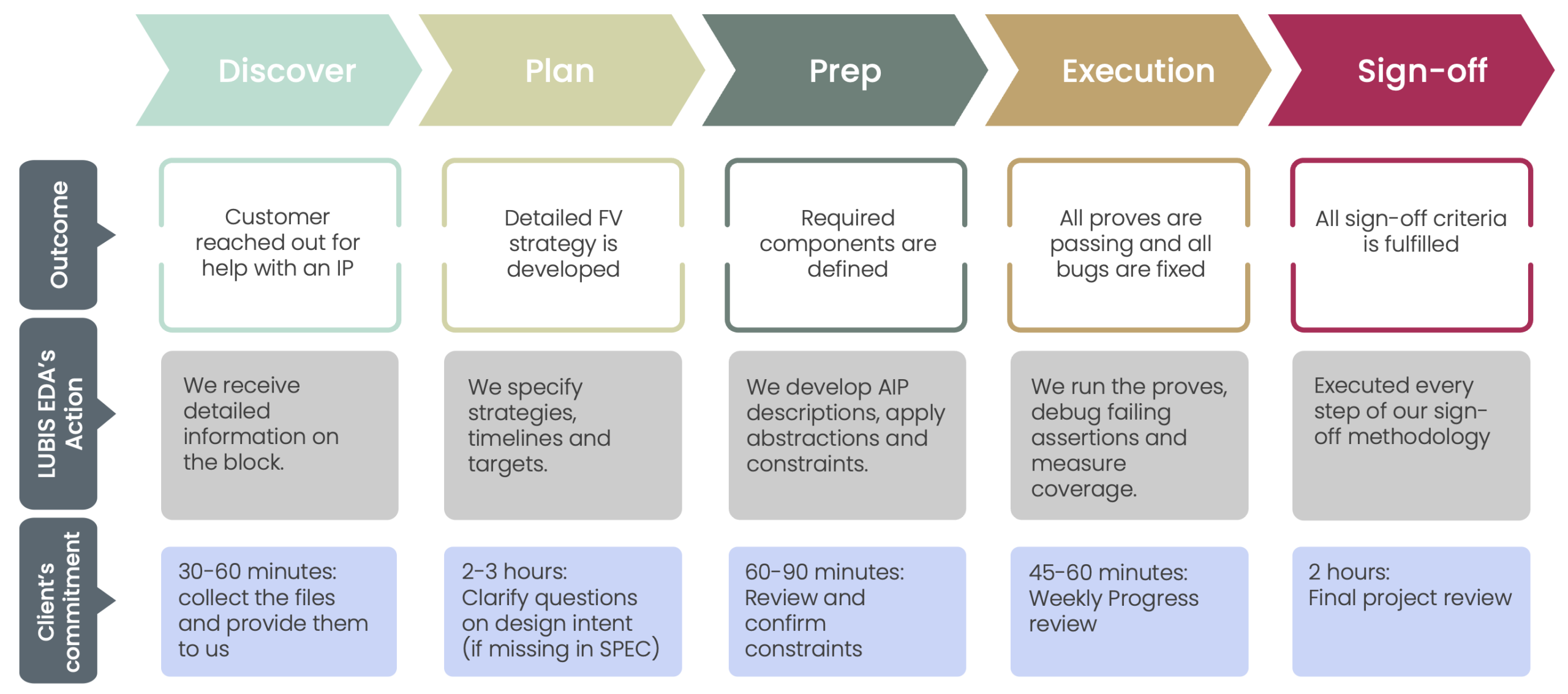
LUBIS EDA is an engineering service provider specialized in formal verification for digital IP blocks and SoCs. The company helps RTL teams reduce schedule risks and uncover simulation-resistant corner-case bugs that are difficult to reach with classical testbench approaches. The offering includes Formal Verification Sign-Off as a service: definition of the Sign-Off plan and scope, property plan with an Assumptions and Constraints approach, coverage and convergence tracking, results documentation, and reusable verification artifacts. The Delivery Model follows a systematic process of Discover, Plan, Prep, Execute and Sign-off; in addition, formal verification results are integrated into customers' regression flows. The team of more than 50 full-time employees works entirely in Germany and has tool expertise in Cadence, Synopsys, and Siemens EDA environments. Two engagement models are offered: Fixed (scope-based, turn-key sign-off) and Subscription (time-based with guaranteed capacity). Customers include five Fortune-25 corporations as well as more than 15 repeat customers.
- Site
- Germany (Headquarters)
- Processes
- Formal Verification Sign-Off (digital circuit/IP verification as a service), Formal Verification Sign-Off for digital IP and SoCs, Formal sign-off plan and scope definition, Property plan and Assumptions/Constraints approach, Coverage and convergence tracking, Results documentation / Sign-Off report, Reusable verification artifacts, Integration of formal verification results into regression flows
- Materials
- Formal Verification Sign-Off, Property Plan & Assumptions/Constraints, Coverage & Convergence Tracking, Sign-Off Report & Artifacts
- Certificates
- Formal Sign-Off report, Coverage & Convergence Tracking
- Employees
- 50+
- Industries
- Semiconductors / EDA, Digital IP and SoC design, Fortune-25 customers (largest global corporations)
- 01
Discover (review of documentation, specification, architecture and
- 02
Plan (verification goals, risks, abstractions, milestones)
- 03
Prep (environment, assumptions, constraints, workflows)
- 04
Execute (properties, debugging, abstraction, coverage)
- 05
Sign-off (evidence evaluation, Sign-Off report)
- 06
Integration into customer regression flows
Processes & Tool Environment
Formal Verification Sign-Off
Structured sign-off of critical digital IP blocks and subsystems with defined criteria and documented evidence.
Property Plan & Assumptions/Constraints
Systematic approach for properties, assumptions, and constraints to secure proofs and convergence.
Coverage & Convergence Tracking
Continuous tracking of coverage and proof convergence up to the agreed sign-off target.
Sign-Off Report & Artifacts
Documentation of results as well as reusable verification artifacts and integration into regression flows.
Locations
Germany (Headquarters)
DEHeadquarters / Engineering Team
- Cadence EDA tooling
- Synopsys EDA tooling
- Siemens EDA tooling
Services
Inside the production
Industries
Processes & technical limits
| Processes | Tolerance | Max. part | Weight | Lot size | Materials |
|---|---|---|---|---|---|
| Formal Verification Sign-Off (digital circuit/IP verification as a service)Engineering | – | – | – | – | – |
Additional services
Reference customers
Quality & Traceability
The sign-off is based on a structured, verifiable evidence collection: scope, validated assumptions, proof status per property, coverage argument, documented abstractions, residual risks, and a register of known gaps. This enables traceability even for stakeholders who did not perform the verification themselves.
| Evidence | Germany (Headquarters) |
|---|---|
| Formal Sign-Off report | |
| Coverage & Convergence Tracking |
History
Over 6 years of company track record
325+ completed Formal-Verification projects with 900+ design bugs uncovered after UVM