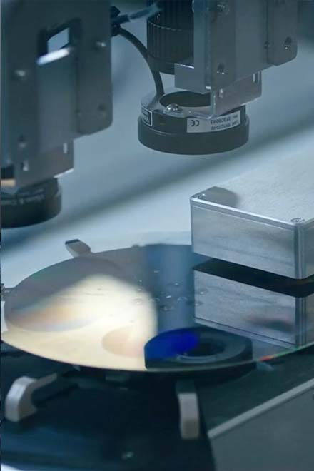
Manufacturing of waveguide optics and display systems for AR glasses – from simulation to series production
Magic Leap, Inc.
Plantation, FL (USA)New on Amplifa
About Magic Leap
Magic Leap, Inc. is a US technology company founded in 2010 and headquartered in Plantation, Florida, specializing in see-through augmented reality. The company manufactures transparent waveguides – ultra-thin optical components that overlay digital content onto the physical world – as well as complete display systems for AR glasses. The value chain covers waveguide design and simulation, materials research, prototyping of AR glasses (including 3D printing, CNC parts and electronics prototyping) and scalable series manufacturing. The core process is the proprietary Jet and Flash Imprint Lithography (J-FIL®) on in-house developed Lithoflex machines, which create nanoscale structures with droplet sizes down to one trillionth of a liter in a single imprint step. Materials used include high-index glass, polymer substrates, silicon carbide and lithium niobate, as well as a proprietary high-refractive-index photoresist. Magic Leap works with global technology corporations such as Google, AT&T, Lucasfilm/ILMxLAB and NTT Docomo, taking partners from patterns through pilot runs to series production. Products also include the AR headsets Magic Leap One (2018) and Magic Leap 2 (2022).
- Site
- Plantation, FL, USA
- Processes
- Jet and Flash Imprint Lithography (J-FIL®) – nanoimprint lithography, Material Etching (etching of nanoscale structures into optical coatings), Surface Planarization (spin-coat layer), UV Curing (UV curing of coatings and waveguide elements), Waveguide Production / Waveguide Manufacturing, Design Engineering / Waveguide Design & Simulation, AR Glasses Prototyping (concept to functional prototype), Rapid Fabrication (3D printing and CNC-machined parts for prototypes)
- Materials
- High-Index Glass, Silicon Carbide (crystalline substrate), Lithium Niobate (crystalline substrate), Polymers (high-index polymer substrates), Proprietary high-refractive-index photoresist (custom-formulated), Jet and Flash Imprint Lithography, Lithoflex Platform, High-Index Polymer Substrates
- Certificates
- ISO/IEC 27001:2022, ISO/IEC 27001:2022 (Information Security)
- Founded
- 2010
- Industries
- Augmented Reality, Consumer Electronics, Entertainment (Gaming/Media), Enterprise/Industrial AR, Military (Historical), Military (Historical: Chosen Realities)
- 01
Waveguide Design & Simulation
- 02
Materials Research & Material Development
- 03
Wafer Preparation & Optical Coating
- 04
J-FIL® Nanoimprint (Lithoflex)
- 05
UV Curing
- 06
Material Etching
- 07
Surface Planarization
- 08
Metrology & In-Process Inspection
- 09
Display System Integration
- 10
Prototyping & Validation
- 11
Scale-Up to Series Production
Materials & Processes
Jet and Flash Imprint Lithography
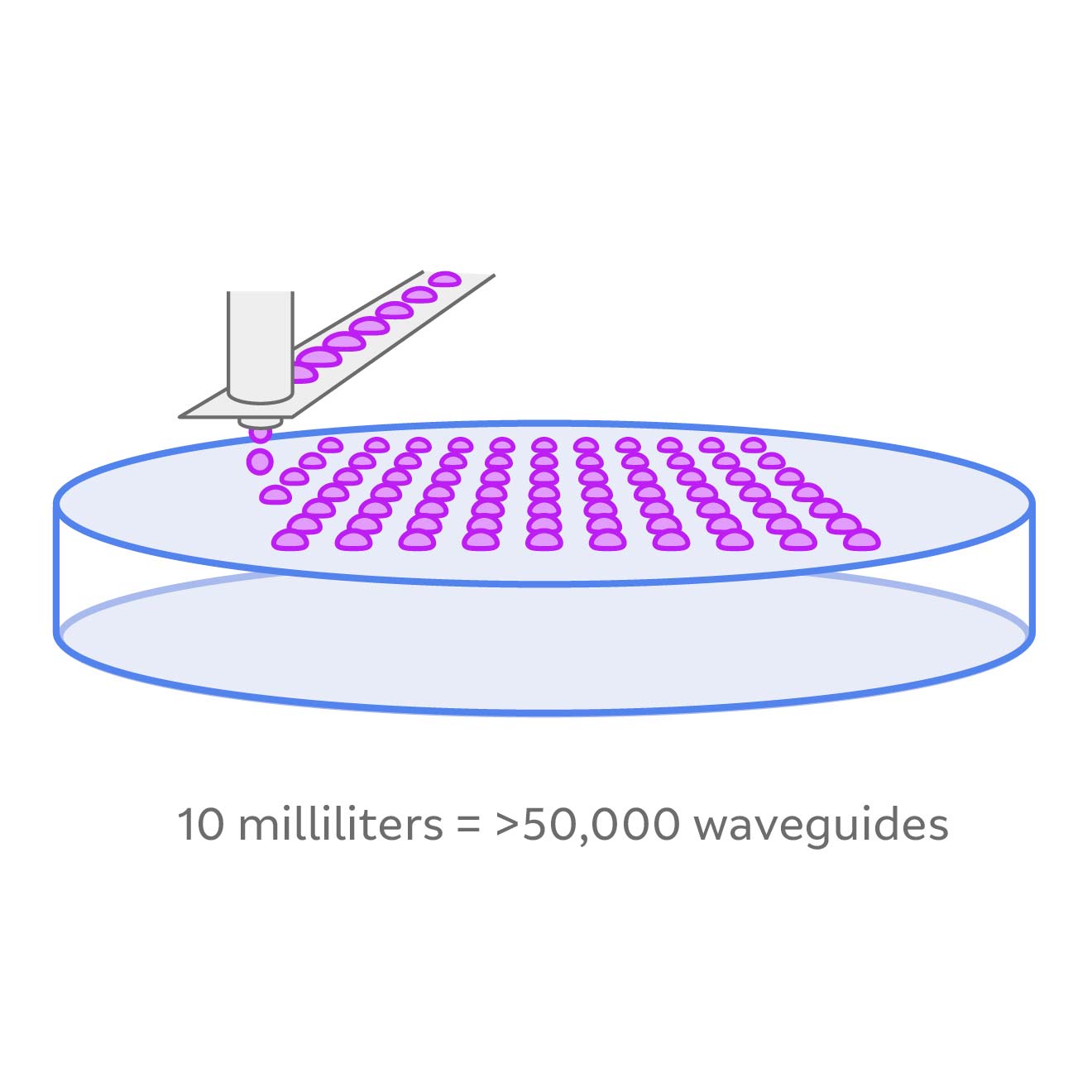
Proprietary nanoimprint process that creates complex nanoscale 3D structures with depth gradation in a single imprint step.
Lithoflex Platform
In-house developed nanoimprint machines for precise droplet dispensing down to one trillionth of a liter and controlled pattern transfer.
High-Index Glass
Optical glass with a high refractive index, compatible with established supply chains and therefore practical for scalable waveguide production.
Silicon Carbide (crystalline substrate)
Durable, thermally stable crystalline substrate with optical properties that enable field-of-view capabilities of 50 degrees or more.
Lithium Niobate (crystalline substrate)
More affordable crystalline material with optical benefits similar to silicon carbide, though more brittle.
High-Index Polymer Substrates
Polymer substrates that reduce the weight of waveguides and provide the durability required for everyday devices.
High-Refractive-Index Photoresist (proprietary)
Proprietarily formulated photoresist specifically tailored to the J-FIL® process for precise waveguide structures.
Surface Planarization
Spin-coat layer that creates a smooth optical surface and reduces visual artifacts such as rainbow effects.
UV Curing
UV curing systems for fast, precise bonding of coatings and waveguide elements.
Rapid Fabrication
3D printing and CNC-machined parts for rapid prototype iterations of fit, function and comfort.
Locations
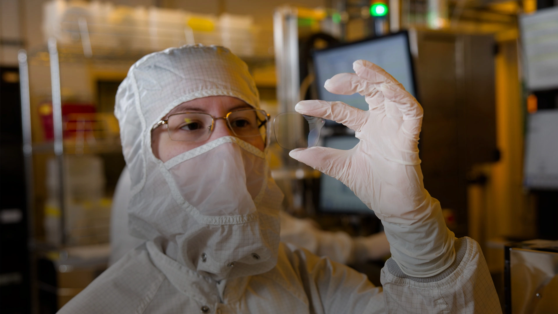
Plantation, FL
USHeadquarters, waveguide production, prototyping and quality assurance
- Lot size
- Samples and pilot runs through series production
- Materials
- High-index glass, silicon carbide, lithium niobate, polymers, photoresist
- Lithoflex nanoimprint machines (J-FIL®)
- High-resolution camera defect scan systems
- Waveguide evaluation machines (nanometer range)
- UV curing systems
- Eyepiece evaluation devices (internally developed)
- Integrated test and inspection tools
- Robotic and optical test systems
- Audio lab
- 3D printing and CNC manufacturing for prototypes
Components
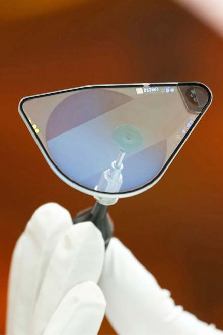

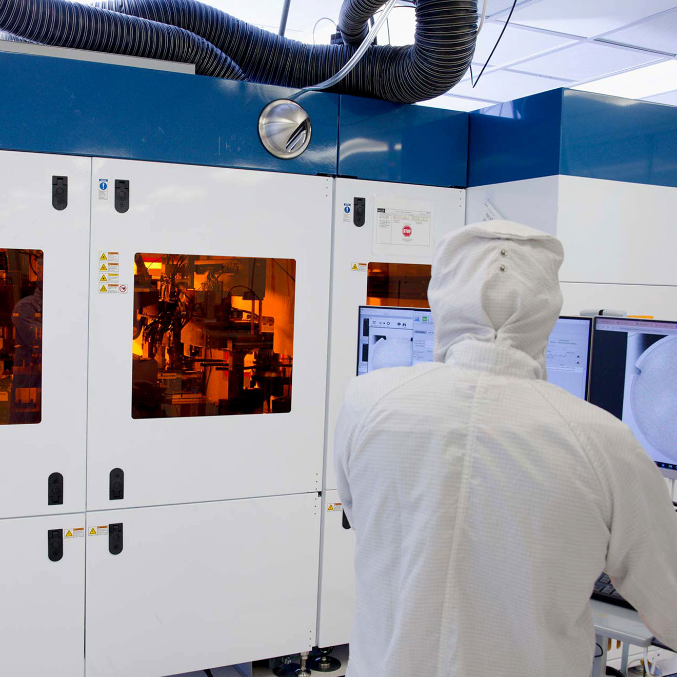
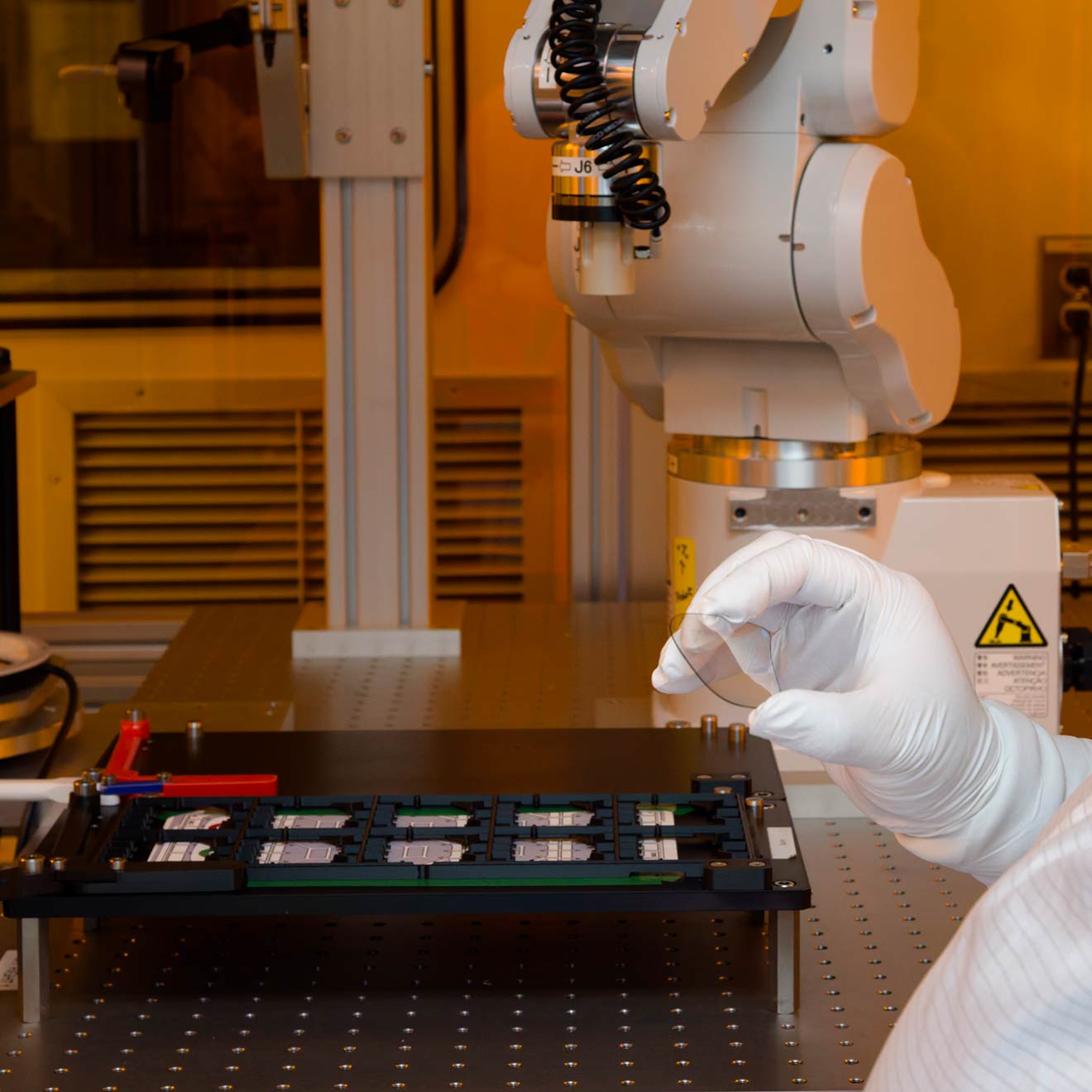
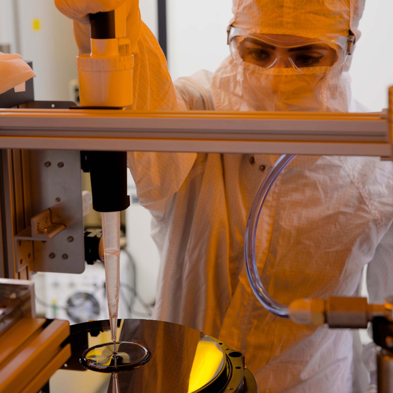
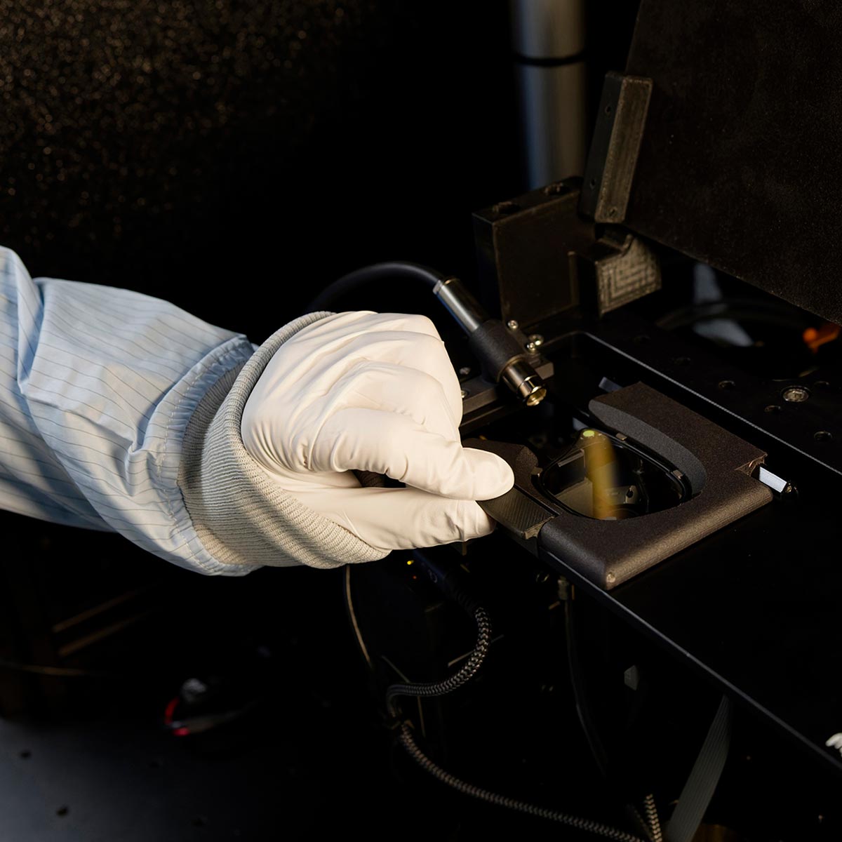
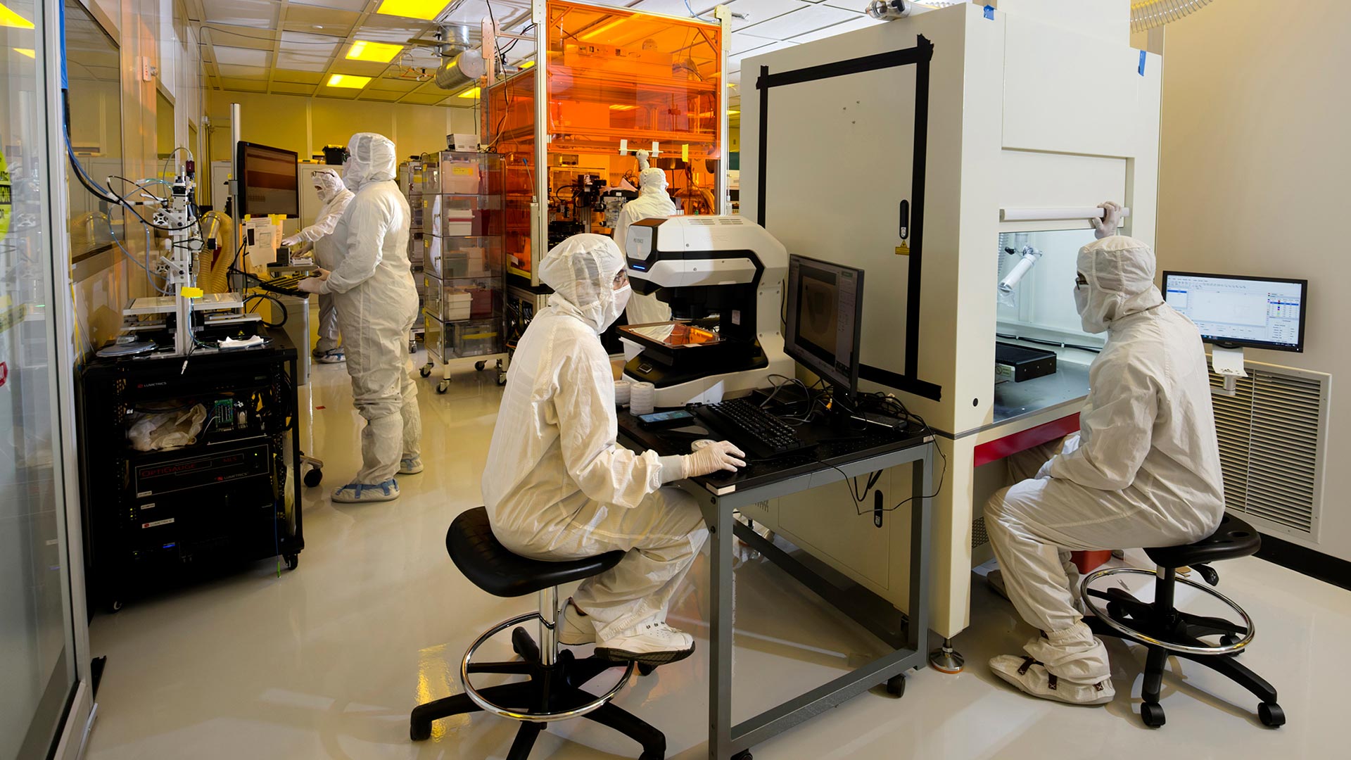
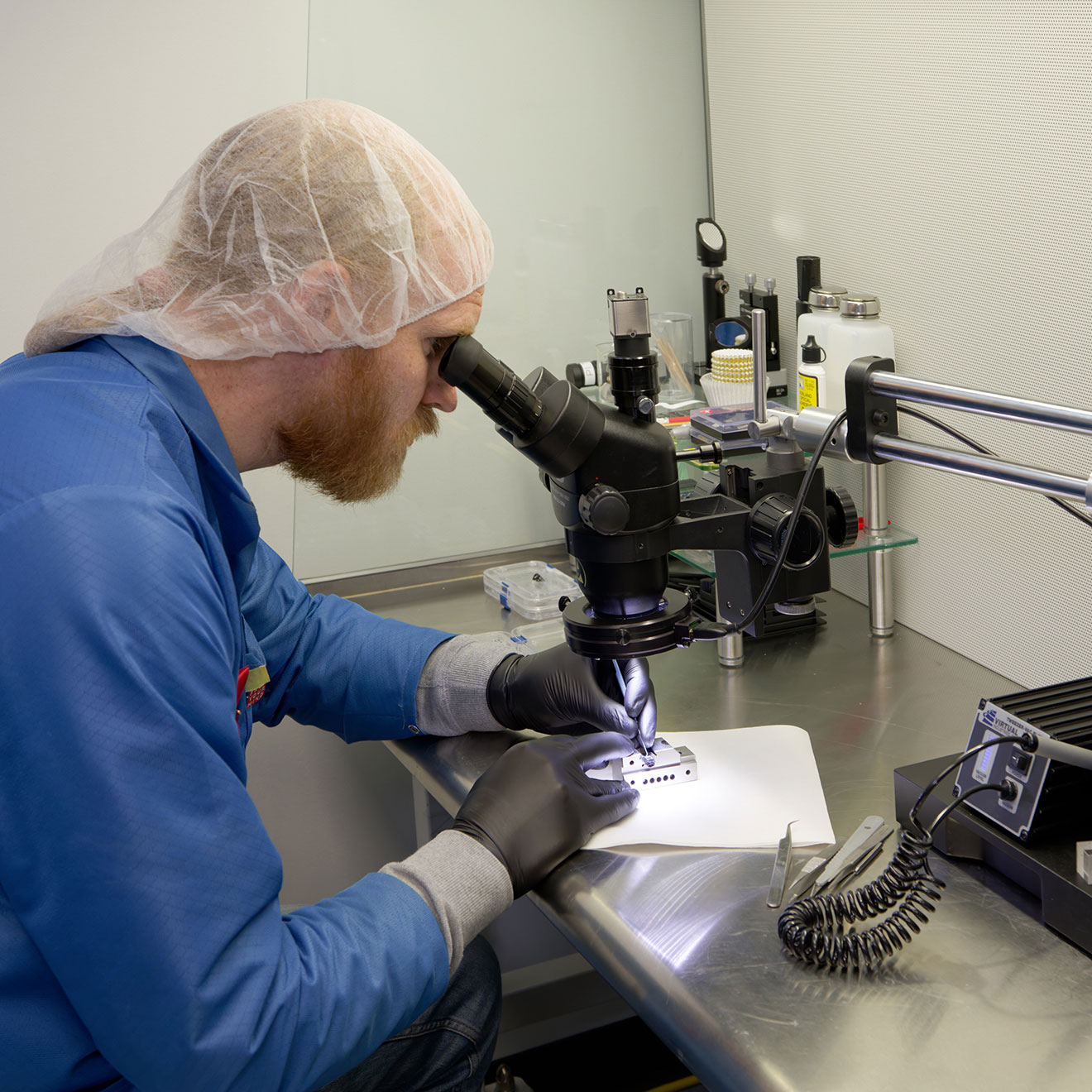
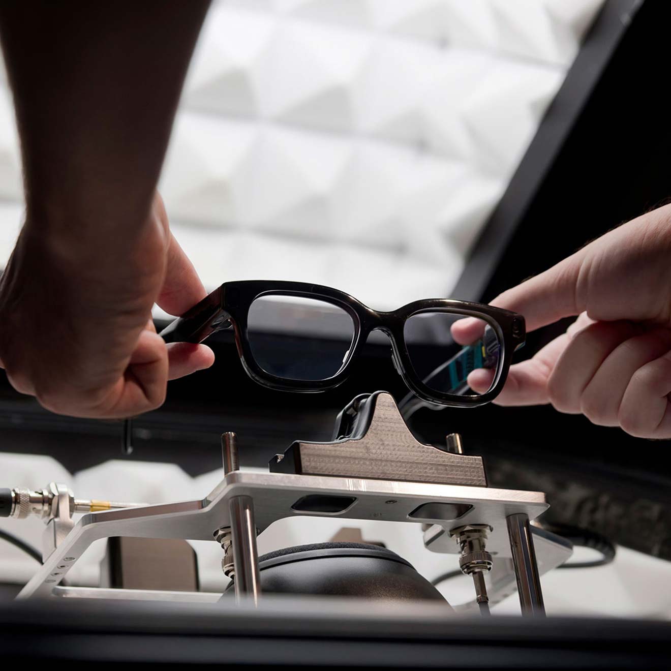
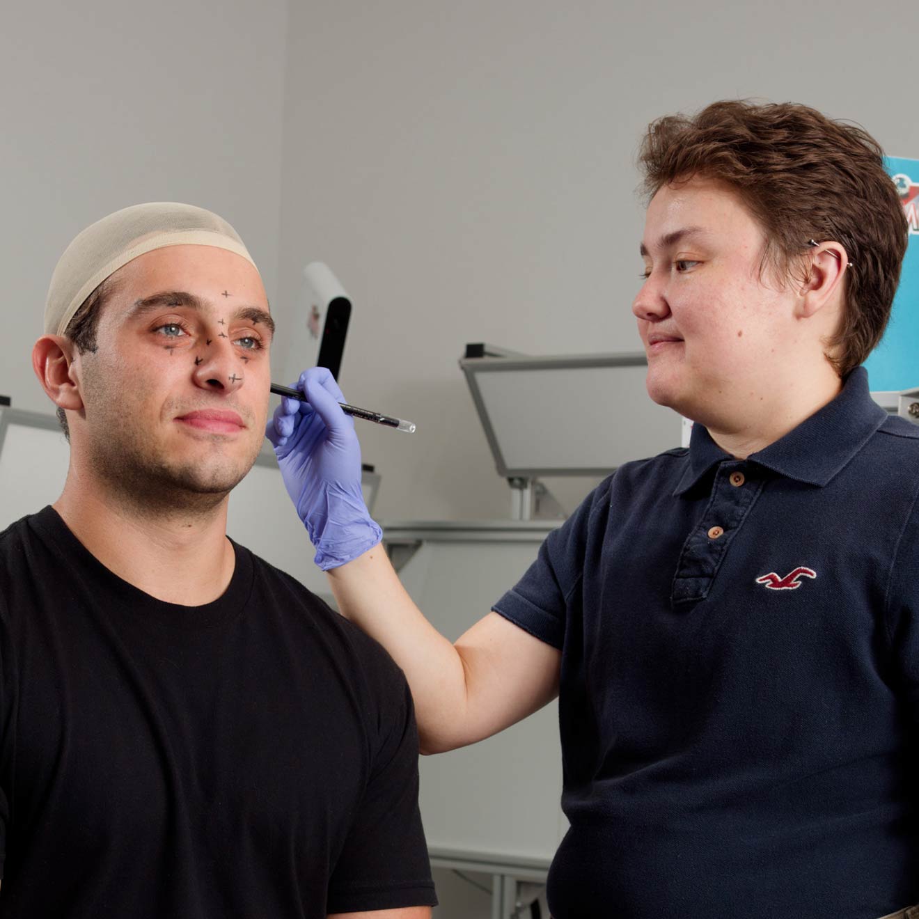
Inside the production
Industries
Processes & technical limits
| Processes | Tolerance | Max. part | Weight | Lot size | Materials |
|---|---|---|---|---|---|
| Jet and Flash Imprint Lithography (J-FIL®) – nanoimprint lithographyPlastics | – | – | – | – | high-refractive index photoresist, high index glass, Polymers |
| Material Etching (etching of nanoscale structures into optical coatings)Surface | – | – | – | – | high index glass, Silicon carbide, Lithium niobate |
| Surface Planarization (spin-coat layer)Surface | – | – | – | – | Photoresist, Polymers |
| UV Curing (UV curing of coatings and waveguide elements)Joining | – | – | – | – | Photoresist |
| Waveguide Production / Waveguide ManufacturingEngineering | – | – | – | Samples and pilot runs – Series production | high index glass, Silicon carbide, Lithium niobate, Polymers, Photoresist |
| Design Engineering / Waveguide Design & SimulationEngineering | – | – | – | – | high index glass, Silicon carbide, Polymers |
| AR Glasses Prototyping (concept to functional prototype)Engineering | – | – | – | – | – |
| Rapid Fabrication (3D printing and CNC-machined parts for prototypes)Additive | – | – | – | – | – |
| Electronics Prototyping (circuits and boards)Assembly | – | – | – | – | – |
| Validation Testing (stress, drop and thermal tests, accelerated aging)Testing | – | – | – | – | – |
| Metrology and Testing (pattern, optical and yield inspection in the nanometer range)Testing | Measurement down to the nanometer range | – | – | – | – |
| Quality Assurance / In-Process Checks (material, assembly and performance inspection)Testing | – | – | – | – | – |
| Usability and User Experience Testing (motion tracking, depth perception, comfort assessment)Testing | – | – | – | – | – |
| Audio Lab Testing (spatial sound, acoustics tuning)Testing | – | – | – | – | – |
| Display System IntegrationAssembly | – | – | – | – | – |
7 Anlagen & Maschinen
| Machine | Manufacturer / model | Quantity | Working area | Year built | Site |
|---|---|---|---|---|---|
| Lithoflex – proprietary nanoimprint machine (Jet and Flash Imprint Lithography) | Magic Leap (proprietary, purpose-built) Lithoflex | – | Droplet dispensing down to one trillionth of a liter; nanoscale structures | – | – |
| High-resolution camera systems for waveguide defect scanning (lightly adapted off-the-shelf | – | – | – | – | – |
| Waveguide evaluation machines (measurement in the nanometer range) | – | – | – | – | – |
| UV curing systems (precise, fast bonding of coatings) | – | – | – | – | – |
| Custom measuring devices for evaluating eyepiece image transmission to the eye | Magic Leap (internally developed) | – | – | – | – |
| Integrated test and inspection tools in waveguide manufacturing (custom-built, create and | Magic Leap (proprietary) | – | – | – | – |
| Robotic tools and optical test systems (automated verification) | – | – | – | – | – |
Additional services
Reference customers
Quality
Quality assurance is integrated into every step at Magic Leap: proprietary, custom-built machines create and inspect components at the same time, metrology measures down to the nanometer range, and every wave is evaluated against the TRUE KPIs (Transmission, Reflectivity, Uniformity, Efficiency). In addition, prototypes undergo stress, drop and thermal testing as well as accelerated aging, complemented by usability tests covering motion tracking, depth perception and wearing comfort.
| Evidence | Plantation, FL |
|---|---|
| ISO/IEC 27001:2022 (Information Security) |
History
- 2010
Founded by Rony Abovitz
- 2014
Over USD 540 million in venture capital from Google, Qualcomm, Andreessen Horowitz, Kleiner Perkins and others
- 2016
Partnership with Lucasfilm/ILMxLAB; acquisition of NorthBit
- 2017
Acquisition of Dacuda's 3D division; company valuation approx. USD 8 billion
- 2018
Magic Leap One launched exclusively via AT&T; AT&T as investor and partner; acquisition of Chosen Realities
- 2019
Acquisition of Mimesys; USD 280 million from NTT Docomo
- 2020
Restructuring with roughly 50% workforce reduction; USD 350 million in new funding; Peggy Johnson becomes new CEO
- 2021
USD 500 million in funding; valuation approx. USD 2 billion
- 2022
Market launch of the Magic Leap 2 on September 30
- 2023
Ross Rosenberg becomes CEO
- 2024
Partnership with Google; around 75 positions cut; cumulative funding of at least USD 3.5 billion
- 2024
End-of-life of cloud services for Magic Leap 1