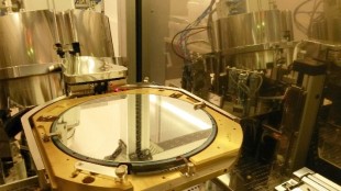
Wafer-level components made of structured, low-temperature-deposited glass for UV LEDs, laser diodes and sensors.
MSG Lithoglas GmbH
Dresden (Headquarters) · Berlin (Branch Office)New on Amplifa
About MSG Lithoglas
MSG Lithoglas GmbH develops, manufactures and distributes wafer-level components of high optical quality based on a patternable low-temperature glass deposition technology. The product portfolio comprises Windows, Mirror and Cavity Caps for wafer-level or COB packaging, hermetic SMD glass encapsulations for UV LEDs and LED arrays, as well as UVC LED modules in a proprietary reflector packaging technology with output up to 2 W in the wavelength range 265–280 nm. Bonding capabilities include aligned and non-aligned bonding using anodic bonding, direct bonding and adhesive bonding on state-of-the-art equipment. The components are characterized by high light output, excellent thermal behavior and high reliability. Customers include the UV LED, laser diode, optical sensor, image sensor and UV disinfection (UVC) industries. The company is represented in the DACH region with its headquarters in Dresden (Maria-Reiche-Str. 1) and a branch office in Berlin (Gustav-Meyer-Allee 25) and was awarded 3rd place and a state prize at the 2023 Saxon Innovation Conference.
- Site
- Dresden
- Processes
- Anodic Bonding, Direct Bonding, Adhesive Bonding, Wafer-Level Glass Deposition (low-temperature glass deposition), Manufacture of Wafer-Level Components (Windows, Mirror, Cavity Caps), Glue Bonding, Wafer-Level Packaging, Hermetic SMD Glass Encapsulation / Capping
- Materials
- Glass (low-temperature depositable, structured glass), Structured Low-Temperature Glass, Anodic Bonding, Direct Bonding, Adhesive Bonding, Wafer-Level Packaging, Reflector Packaging
- Industries
- UV LED, Laser Diodes, Optical Sensor Technology, Image Sensor Technology, UV Disinfection (UVC), Laser Diodes
- 01
Glass deposition (low-temperature, structured)
- 02
Structuring at wafer level
- 03
Bonding (anodic, direct, adhesive)
- 04
Wafer-level packaging / hermetic SMD glass encapsulation
- 05
Assembly including UVC LED module manufacturing
Materials & Processes
Structured Low-Temperature Glass
Depositable, patternable glass as the base material for optical wafer-level components and hermetic glass encapsulations.
Anodic Bonding
Aligned and non-aligned anodic bonding of glass for hermetic capping solutions.
Direct Bonding
Direct bonding for optically high-quality, reliable wafer bonds.
Adhesive Bonding
Adhesive bonding as a complementary joining technique for capping applications.
Wafer-Level Packaging
Hermetic SMD-type glass encapsulation of UV LEDs and arrays at wafer level.
Reflector Packaging
Proprietary packaging technology for high-power UVC LED modules with up to 2 W optical output power.
Sites
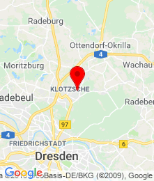
Dresden
DEHeadquarters
- Materials
- Glass
- Systems for anodic, direct and adhesive bonding
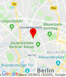
Berlin
DEBranch Office
Components & Products
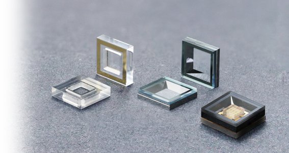
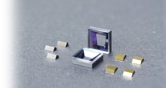
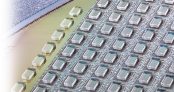
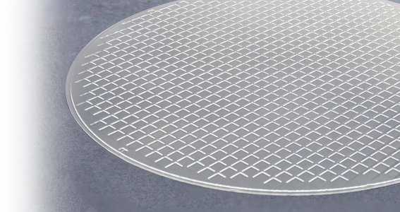
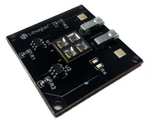
Inside the production

Industries
Processes & technical limits
| Processes | Tolerance | Max. part | Weight | Lot size | Materials |
|---|---|---|---|---|---|
| Anodic BondingJoining | – | – | – | – | Glass |
| Direct BondingJoining | – | – | – | – | Glass |
| Adhesive BondingJoining | – | – | – | – | Glass |
| Wafer-Level Glass Deposition (low-temperature glass deposition)Additive | – | – | – | – | Glass |
| Manufacture of Wafer-Level Components (Windows, Mirror, Cavity Caps)Assembly | – | – | – | – | Glass |
Additional services
History
- 2023
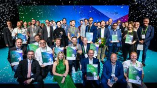
3rd place and state prize at the Saxon Innovation Conference in Dresden (July 4, 2023).