EU-funded Horizon 2020 research project for the development of modeling and simulation tools for nanoscaled semiconductor devices

MUNDFAB – Modeling Unconventional Nanoscaled Device FABrication
Erlangen (Fraunhofer IISB, Schottkystraße 10)New on Amplifa
About the project
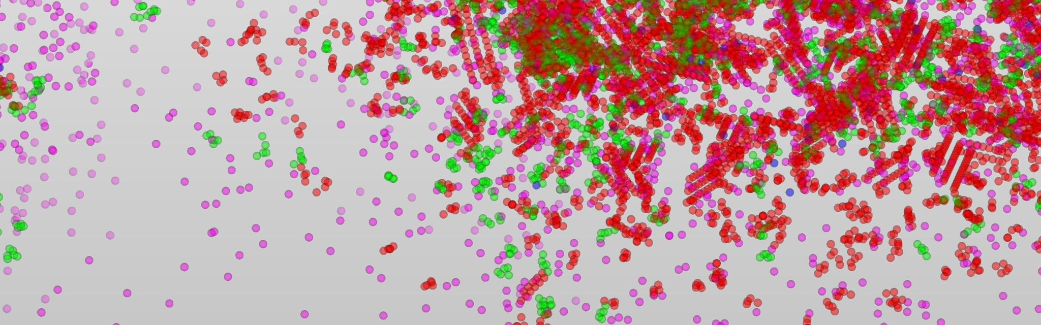
MUNDFAB (Modeling Unconventional Nanoscaled Device FABrication) is a research project funded by the EU under Horizon 2020 (Grant Agreement No. 871813) with a duration from 01.01.2020 to 30.06.2023. Project coordination was based at Fraunhofer IISB in Erlangen. The aim of the project was the development of modeling and simulation tools (KMC, DFT, TCAD/Synopsys Sentaurus) for the virtual fabrication of the next generation of nanoscaled electronic devices, in particular based on 3D sequential integration architectures. The consortium comprised Fraunhofer IISB, CNR, CEA-Leti, CNRS, STMicroelectronics, TU Wien and Łukasiewicz-IMiF, as well as Applied Materials as a partner. Experimental work investigated, among other things, CVD epitaxy (Si, SiGe), heated ion implantation, sub-melt laser annealing, SPER and silicidation, and translated the findings into process models. Results fed into demonstrators such as FDSOI devices and vertical GAA nanowire FETs.
- Site
- Erlangen
- Processes
- CVD epitaxy (Si, SiGe, in-situ doped), Ion implantation (heated implants, As/B/P), Sub-melt laser annealing (µs-LA, KrF/XeCl pulsed), Solid Phase Epitaxy Regrowth (SPER), Silicidation (Si-Ni, Si-Pt), Thermal oxidation of silicon, Silicon etching, Characterization: SIMS, TEM, XRD, XRR, spectroscopic ellipsometry, 4-point probe, Hall effect,
- Materials
- Silicon, Silicon-germanium, Germanium, Silicon dioxide, Silicon nitride, Silicon-germanium oxide, Nickel silicide, Platinum silicide
- Industries
- Semiconductors, Micro-/nanoelectronics, Research
- 01
Ab-initio calculations (DFT)
- 02
Experimental process development (epitaxy, implantation, laser annealing,
- 03
Calibration of KMC process models
- 04
Integration into TCAD toolchains (Synopsys Sentaurus)
- 05
Demonstrators and validation
Materials and processes
Silicon
Base material for epitaxy, implantation, oxidation and silicidation.
Silicon-germanium
Strained, in-situ boron-doped layers for epitaxy and laser annealing experiments.
Germanium
Semiconductor material in epitaxy processes with germane precursor.
Silicon dioxide
Subject of thermal oxidation and defect simulations.
Silicon nitride
Investigated with regard to intrinsic charge trapping.
Silicon-germanium oxide
Investigated with regard to oxygen vacancies and defect states.
Nickel silicide
Silicidation product in the Si-Ni system.
Platinum silicide
Silicidation product in the Si-Pt system.
Locations
Erlangen
DEProject coordination (Fraunhofer IISB)
- Materials
- Silicon, SiGe
Inside the production
Industries
Processes & technical limits
| Processes | Tolerance | Max. part | Weight | Lot size | Materials |
|---|---|---|---|---|---|
| CVD epitaxy (Si, SiGe, in-situ doped)Additive | – | – | – | – | Silicon, SiGe, Germanium |
| Ion implantation (heated implants, As/B/P)Surface | – | – | – | – | Silicon, SiGe |
| Sub-melt laser annealing (µs-LA, KrF/XeCl pulsed)Heat treatment | – | – | – | – | SiGe:B, Silicon |
| Solid Phase Epitaxy Regrowth (SPER)Heat treatment | – | – | – | – | Silicon, SiGe |
| Silicidation (Si-Ni, Si-Pt)Joining | – | – | – | – | Silicon, Nickel, Platinum |
| Thermal oxidation of siliconSurface | – | – | – | – | Silicon, SiO2 |
| Silicon etchingSurface | – | – | – | – | Silicon |
| Characterization: SIMS, TEM, XRD, XRR, spectroscopic ellipsometry, 4-point probe, Hall effect,Testing | – | – | – | – | Silicon, SiGe, SiO2 |
5 Anlagen & Maschinen
| Machine | Manufacturer / model | Quantity | Working area | Year built | Site |
|---|---|---|---|---|---|
| Epitaxy reactor | Applied Materials CENT300A | 1 | – | 2021 | – |
| Epitaxy reactor | ASM Epsilon 3200A | 1 | – | 2018 | – |
| Pulsed laser annealing (XeCl, 308 nm) | SCREEN-LASSE LT3100 | 1 | Shot 15 x 15 mm² | – | CEA-LETI |
| Pulsed laser (KrF, 248 nm) | COMPex 201F | 1 | Shot 3 x 3 mm² | – | CNR-UNIPD |
| µs laser annealing platform (355 nm UV) | SCREEN LASSE | 1 | Shot 10 x 10 mm² | – | – |
Additional services
Reference customers
Project history
- 2020
Project start of MUNDFAB (Horizon 2020, Grant No. 871813) on 01.01.2020
- 2023
Project end on 30.06.2023; symposium 'Materials Engineering for Advanced Semiconductor Devices' at the E-MRS Spring Meeting in Strasbourg