Manufacturer of custom quartz, glass and LT/LN wafers as well as precision optics with production in Langenzenn

Nano Quarz Wafer GmbH
Langenzenn (90579) · DENew on Amplifa
About Nano Quarz Wafer
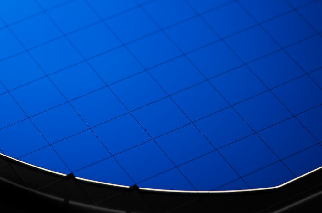
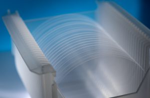
Nano Quarz Wafer GmbH (NQW) is a manufacturer of custom quartz, glass, lithium tantalate (LT) and lithium niobate (LN) wafers as well as precision optics, headquartered in Langenzenn near Nuremberg. The product range includes fused silica, glass, crystal quartz, Si, SOI and SiC wafers as well as optical filters and thin-film coatings such as Anti-Reflective, High-Reflective, metal, ITO and FTO coatings. In addition to the production of new bare wafers, the company offers reclaim and processing services, including single- and double-side grinding, lapping and polishing (down to 100 µm thickness), cleaning, etching, downsizing, laser marking according to SEMI M1, and CNC edge polishing. Production takes place in a Class 4–6 cleanroom environment; wafers are manufactured from 2" to 300 mm in diameter and from 100 µm to 10 mm in thickness, polished to Ra < 0.5 nm. Customer industries include microsystems technology, medical technology, the laser industry, telecommunications, the semiconductor and optics industries, as well as OLED production and SAW/telecom applications. Via distribution partners, NQW delivers to Europe, the USA, Singapore, China and Taiwan.
- Site
- Langenzenn
- Processes
- Wafer manufacturing (bare wafers) / Wafer Technology, Thin Film Coating (Anti-Reflective, High-Reflective, metal, ITO), Reclaim Processing (Grinding, Lapping, Polishing, Etching, Downsizing, Laser Marking), Single & Double Side Polishing, Grinding (double or single side, front-/backside grinding down to 100 µm), Lapping (double or single side), Etching Service, CMP & Reclaim process for LT/LN wafers
- Materials
- Fused Silica (quartz glass), Glass Wafer, Borofloat33, Lithium tantalate (LT, LiTaO3), Lithium niobate (LN, LiNbO3), Crystal Quartz, Silicon Wafer, SOI Wafer
- Certificates
- Integrated management system with wafer tracking
- Industries
- Microsystems Technology, Medical Technology, Laser Industry, Telecommunications, Semiconductor Industry, Optics Industry
- 01
Substrate cutting (glass/crystal)
- 02
Grinding / Lapping
- 03
Polishing (single-/double-sided)
- 04
Cleaning & Etching
- 05
Thin-film coating
- 06
Laser marking
- 07
Metrology / Inspection
Sites
Langenzenn
DEHeadquarters, Production, Research & Development
- Part weight / size
- 2" – 300 mm diameter
- Lot size
- Small evaluation/development series up to High Volume Production
- Materials
- Fused Silica, glass, Borofloat33, Crystal Quartz, LT, LN, Si, SOI, SiC, filter glass
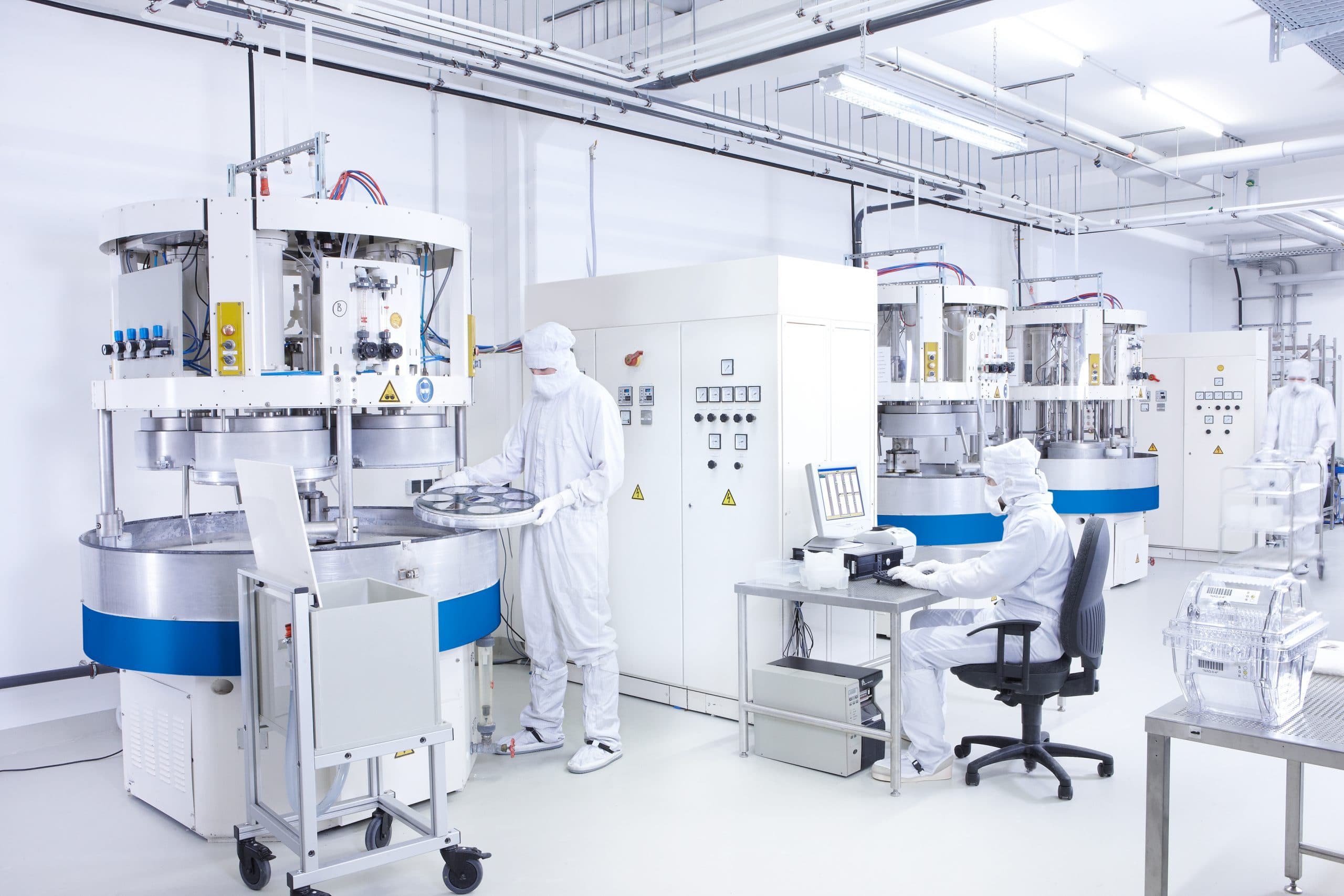
- Class 4–6 cleanroom
- KEYENCE 3D laser scanning microscope (2025)
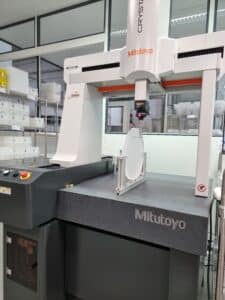
- Mitutoyo 3D coordinate measuring machine
- Polishing machines
- Semiconductor standard cleaning system
Components & Products
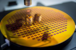
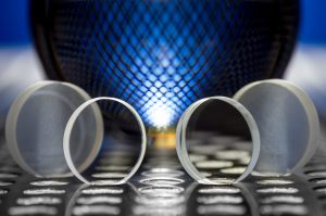
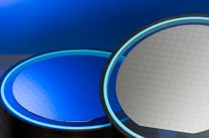
Inside the production
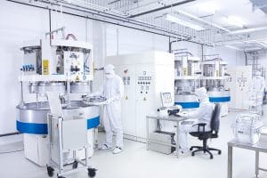

Industries
Processes & technical limits
| Processes | Tolerance | Max. part | Weight | Lot size | Materials |
|---|---|---|---|---|---|
| Wafer manufacturing (bare wafers) / Wafer TechnologyEngineering | TTV (GBIR) < 2 µm; Bow/Warp < 20 µm; LTV < 0.4 µm (5×5 mm²) · Ra < 0.5 nm polished (AFM), Ra 0.1–2.0 | Diameter 2" to 300 mm × Thickness 100 µm to 10 mm | – | small evaluation/development series – High Volume Production | Fused Silica, Glass, LT (LiTaO3), LN, Crystal Quartz, Si, SOI, SiC |
| Thin Film Coating (Anti-Reflective, High-Reflective, metal, ITO)Surface | – | Optics up to 12" diameter | – | – | Fused Silica, Low Expansion Glass, Filter Glass, Glass, ITO glass, FTO glass, ITO-PET |
| Reclaim Processing (Grinding, Lapping, Polishing, Etching, Downsizing, Laser Marking)Surface | – | 2" – 300 mm × Front-/backside grinding down to 100 µm | – | – | Fused Silica Wafer, SiC Wafer, Silicon Wafer, Glass Wafer (Borofloat33), Quartz Crystal, LT (LiTaO3), LN (LiNbO3) |
| Single & Double Side PolishingSurface | Ra < 0.5 nm (polished) | 2" – 300 mm | – | – | Fused Silica, Glass, Quartz, Si, SiC, LT, LN |
| Grinding (double or single side, front-/backside grinding down to 100 µm)Machining | – | 2" – 300 mm | – | – | Fused Silica, Glass, Quartz, SiC, Si, LT, LN |
| Lapping (double or single side)Surface | – | 2" – 300 mm | – | – | Glass, Quartz, Fused Silica |
| Etching ServiceSurface | – | 2" – 300 mm | – | – | Fused Silica, Glass, LT, LN |
| CMP & Reclaim process for LT/LN wafersSurface | – | 2" – 300 mm | – | – | Lithium tantalate, Lithium niobate |
| Polyimide film removal from glass wafers (reclaim process)Surface | – | 2" – 300 mm | – | – | Glass (Borofloat33 et al.) |
| Laser marking (T7/OCR, SEMI M1)Surface | – | 2" – 300 mm | – | – | Glass, Quartz, Fused Silica, LT, LN |
| CNC edge polishing and grindingMachining | – | 2" – 300 mm | – | – | Glass, Quartz, Fused Silica |
| Wafer bonding (ZIM PermanentBond, development)Joining | Target: TTV < 2 µm | – | – | – | Glass, Silicon, Lithium tantalate |
| Glass round substrate cuttingMachining | – | up to 12" | – | – | Fused Silica, Glass, Filter Glass |
| Cleaning in semiconductor standard cleaning system / wafer cleaning serviceSurface | – | – | – | – | Fused Silica, Glass, Quartz, Si, LT, LN |
| Optical coating according to DIN ISO 10110 / precision opticsTesting | DIN ISO 10110 | – | – | – | Fused Silica, Glass, Filter Glass |
4 Anlagen & Maschinen
| Machine | Manufacturer / model | Quantity | Working area | Year built | Site |
|---|---|---|---|---|---|
| 3D laser scanning microscope | KEYENCE | 1 | – | 2025 | Langenzenn |
| 3D coordinate measuring machine (CMM) | Mitutoyo | 1 | – | – | Langenzenn |
| Polishing machine | – | – | – | – | Langenzenn |
| Semiconductor standard cleaning system | – | – | – | – | Langenzenn |
Additional services
Quality & Metrology
Production takes place in a Class 4–6 cleanroom environment with an integrated management system and individual wafer tracking (QR code system). Metrology equipment includes a KEYENCE 3D laser scanning microscope (2025) and a Mitutoyo 3D coordinate measuring machine; optical coatings are performed according to DIN ISO 10110.
| Evidence | Langenzenn |
|---|---|
| Integrated management system with wafer tracking |
History
More than 20 years of experience in wafer technology and production
- 2025
Investment in 3D laser scanning microscope (KEYENCE) and 3D coordinate measuring machine (Mitutoyo)
- 2025
ZIM project PermanentBond – innovative wafer bonding for glass/silicon/lithium tantalate composites
- 2025
100 µm thin Borofloat33 and fused silica wafers transferred to production
- 2026
New General Terms and Conditions introduced