NanoWired develops electrochemical NanoWiring and KlettWelding processes for joining metallic substrates without soldering or sintering.

NanoWired GmbH
Gernsheim (HQ) · New Taipei City (TechCenter Asia) · Stains (Sales)New on Amplifa
About NanoWired
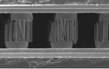
NanoWired GmbH is a technology company founded in 2019 and based in Gernsheim (Hesse), which emerged from the EXIST research transfer grant following the Kick-off in 2015 in Darmstadt. The core of the company is the patented NanoWiring process: an electrochemical process that creates metallic nanostructures (nanoWires) on almost any surface. Based on this, joining technologies such as KlettWelding, KlettSintering and KlettGlueing as well as KlettWelding tapes replace soldering, silver/copper sintering, TLPS and brazing for metallic or metallized substrates. Materials include copper, silver, gold, nickel, zinc and platinum; carriers can be plastic, glass, ceramic, steel, aluminium, brass or semiconductor material. Applications are in semiconductor and electronic packaging (flip chip, die attach, 3D packaging, chiplet integration), power electronics with busbars, and the automotive, aerospace and sensor industries. The headquarters offers over 800 m² with offices, laboratories (spray coater, lithography, plasma cleaner, sintering press, SEM, shear tester) and ISO5–ISO10 cleanrooms; a TechCenter in Taiwan and a sales office in France complete the company.
- Site
- Gernsheim
- Processes
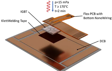
- NanoWiring (electrochemical process for producing metallic nanoWires), KlettWelding (joining two NanoWiring substrates at room temperature, shear strength 6–20 MPa), KlettWelding+ (joining both NanoWiring surfaces, 170–240 °C, shear strength 20–65 MPa), KlettWelding-Underfill (joining with adhesive, low temperature, shear strength approx. 10–50 MPa), KlettSintering (joining with one NanoWiring surface, 170–240 °C, 10–30 MPa, shear strength 20–50, KlettSintering+ (joining with KlettWelding Tape, 170–240 °C, shear strength 30–60 MPa), KlettGlueing (joining with adhesive, 20–150 °C, 1–5 MPa, shear strength approx. 20 MPa), KlettGlueing+ (joining with KlettWelding Tape + adhesive, 20–150 °C, repairable)
- Materials
- Copper, Silver, Gold, Nickel, Zinc, Platinum, Polyimide (insulating material / tape core), Plastic (carrier material)
- Certificates
- ISO 9001:2015, ISO 9001:2015 (DEKRA)
- Founded
- 2019
- Industries
- Semiconductor and electronic packaging, Power electronics, Automotive, Aerospace, Sensor technology
- 01
Engineering & R&D services
- 02
Substrate preparation (cleaning, masking, lithography)
- 03
NanoWiring (electrochemical nanoWire deposition)
- 04
Stripping & cleaning
- 05
Joining (KlettWelding / KlettSintering / KlettGlueing, optionally with tape)
- 06
Pick & Place / assembly (die attach, power module, TIM)
- 07
Testing (SEM, confocal microscopy, shear tester)
Sites

Gernsheim
DEHeadquarters with office, laboratory and ISO5–ISO10 cleanrooms
- Lot size
- Prototype to series
- Materials
- Cu, Ag, Au, Ni, Zn, Pt
- NanoWiring Cube
- Spray Coater
- Lito (lithography)
- Plasma Cleaner
- Laboratory sintering press
- SEM
- Shear Tester
New Taipei City (Xizhi)
TWTechCenter Asia (NanoWired GmbH, Taiwan Branch) – all processes available, network for upstream and analysis processes
Stains
FRSales office (Davum TMC)
Applications & Parts

Inside the production





Industries
Processes & technical limits
| Processes | Tolerance | Max. part | Weight | Lot size | Materials |
|---|---|---|---|---|---|
| NanoWiring (electrochemical process for producing metallic nanoWires)Surface | – | – | – | – | Copper, Gold, Silver, Nickel, Zinc, Platinum |
| KlettWelding (joining two NanoWiring substrates at room temperature, shear strength 6–20 MPa)Joining | – | – | – | – | Copper, Gold, Silver, Nickel |
| KlettWelding+ (joining both NanoWiring surfaces, 170–240 °C, shear strength 20–65 MPa)Joining | – | – | – | – | Copper |
| KlettWelding-Underfill (joining with adhesive, low temperature, shear strength approx. 10–50 MPa)Joining | – | – | – | – | Copper |
| KlettSintering (joining with one NanoWiring surface, 170–240 °C, 10–30 MPa, shear strength 20–50Joining | – | – | – | – | Copper |
| KlettSintering+ (joining with KlettWelding Tape, 170–240 °C, shear strength 30–60 MPa)Joining | – | – | – | – | Copper |
| KlettGlueing (joining with adhesive, 20–150 °C, 1–5 MPa, shear strength approx. 20 MPa)Joining | – | – | – | – | Copper |
| KlettGlueing+ (joining with KlettWelding Tape + adhesive, 20–150 °C, repairable)Joining | – | – | – | – | Copper |
| KlettWelding Tape (adhesive tape/preform with NanoWiring, copper or polyimide core, withoutJoining | – | – | – | – | Copper (5µm, 20µm, 100µm … 2mm), Polyimide (12µm, 25µm, 50µm), Silver, Gold, Nickel |
| Adhesive bonding (adhesive application before low-pressure/low-temperature joining, substitution ofJoining | – | – | – | – | Copper |
| 3D/2D Packaging (chiplet integration, fine-pitch interconnects 5–10µm, 1st-level 40–50µm, 2nd-level)Assembly | – | – | – | – | Copper |
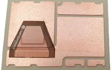
| Power module assembly (Single Step Assembly: NanoWiring on wafer/FPC/DBC, die pick and place)Assembly | – | – | – | – | Copper |
| Die attach / substrate attach (substitution of soldering/sintering/TLPS, die shear strength 50 MPa)Assembly | – | – | – | – | Copper |
| Wire Bonding Replacement / FPCAssembly | – | – | – | – | Copper |
| Thermal Interface Material (TIM) as tape & reel (conductive/insulating)Assembly | – | – | – | – | Copper |
| R&D/services: connection technologies as replacement for soldering, silver/copper sintering and TLPSJoining | – | – | – | – | Copper, Silver, Gold, Nickel |
| Testing/measurement of NanoWiring structures using SEM or confocal microscopyTesting | – | – | – | – | Copper |
7 Anlagen & Maschinen
| Machine | Manufacturer / model | Quantity | Working area | Year built | Site |
|---|---|---|---|---|---|
| NanoWiring Cube (fully automatic NanoWiring system) | NanoWired NanoWiring Cube | – | Production area 400*300 mm, max. substrate height 120 mm | – | Gernsheim / customer facilities |
| Spray Coater | – | – | – | – | Gernsheim (lab) |
| Lito (lithography) | – | – | – | – | Gernsheim (lab) |
| Plasma Cleaner | – | – | – | – | Gernsheim (lab) |
| Laboratory sintering press | – | – | – | – | Gernsheim (lab) |
| SEM (scanning electron microscope) | – | – | – | – | Gernsheim (lab) |
| Shear Tester | – | – | – | – | Gernsheim (lab) |
Additional services
Quality & Certification
NanoWired is certified to ISO 9001:2015 by DEKRA. NanoWiring structures are measured by SEM or confocal microscopy, surfaces are inspected with a stereo microscope; mechanical properties are verified with shear testing.
| Evidence | Gernsheim |
|---|---|
| ISO 9001:2015 (DEKRA) |
History
- 2015
Idea founded – kick-off meeting in Darmstadt, connecting science and industry around the NanoWired concept
- 2019
Company founded as NanoWired GmbH following the EXIST research transfer grant
- 2020
Winner of the Falling Walls Venture Award 2020
- 2021
Technological breakthrough: development of the Lab Machine and first customer installations, international expansion
- 2022
Winner of the TIE Award 2022