
Develops GaN and SiC power semiconductors, driver ICs and system-in-package solutions for efficient power electronics.

NovaWave AG
Biel (Switzerland) · Shenzhen (China)New on Amplifa
About NovaWave
NovaWave is a Swiss provider founded in 2021 of innovative solutions for next-generation wide-bandgap power devices. The company specializes in advanced GaN and driver technologies and offers a portfolio that includes driver ICs for GaN, SiC, IGBTs and MOSFETs, GaN power switches (HEMTs and bare die) as well as complete system-in-package solutions. Added to this are the GaN-on-Si Schottky barrier diode Flash-SBD and the proprietary epitaxy platform GaN-on-QST. NovaWave operates as a fabless company: wafer fabrication of the E-mode GaN power devices is handled by the Korean foundry partner DB HiTek. The headquarters with R&D and design center is located in Biel in the Swiss Innovation Park; an office in Shenzhen ensures worldwide customer support. The products serve applications in consumer electronics, wireless charging, AI and data centers, robotics, industrial power supplies and e-mobility.
- Site
- Biel, Switzerland
- Processes
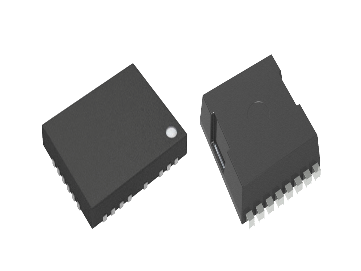
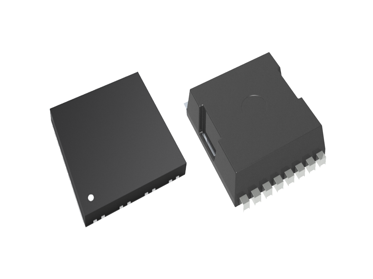
- GaN/SiC power devices and driver solutions, Smart-GaN™ SiP (system-in-package: integrated GaN HEMT and driver IC), Smart-Drive™ IC – driver IC for GaN, SiC, IGBTs and MOSFETs, Flash-SBD™ – GaN-on-Si Schottky barrier diode (2A – 8A), GaN HEMTs and bare die (650V, 100 – 600mΩ Rdson), GaN epitaxial growth (GaN-on-QST platform), Driver ICs for GaN, SiC, IGBTs and MOSFETs, GaN power switches (HEMTs, bare die)
- Materials
- Gallium Nitride (GaN), Silicon Carbide (SiC), Silicon, Gallium nitride (GaN), Silicon carbide (SiC), QST substrate
- Founded
- 2021
- Industries
- Consumer electronics / fast chargers, Wireless charging, Data centers and AI infrastructure, Renewable energies and industrial power supplies, Electric and hybrid vehicles, Robotics and automation
- 01
Device and circuit design (R&D, Biel)
- 02
GaN epitaxy technology (GaN-on-QST)
- 03
Wafer fabrication by foundry partner DB HiTek
- 04
Packaging / system-in-package (SiP)
- 05
Test and validation
- 06
Global customer support (Biel, Shenzhen)
Materials & Technologies
Gallium nitride (GaN)
Wide-bandgap semiconductor for higher switching speeds, lower switching losses and higher power density than silicon.
Silicon carbide (SiC)
Wide-bandgap material for driver ICs and power applications in industrial electronics.
Silicon
Substrate material for the GaN-on-Si Schottky barrier diodes (Flash-SBD).
QST substrate
Substrate platform for the proprietary GaN epitaxy technology GaN-on-QST.
Sites
Biel
CHHeadquarters, R&D and design center in the Swiss Innovation Park
- Materials
- GaN, SiC
Shenzhen
CNOffice for global customer support
Products & Devices
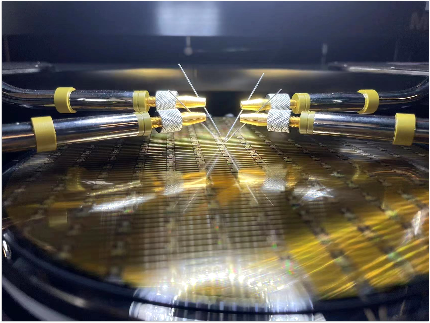
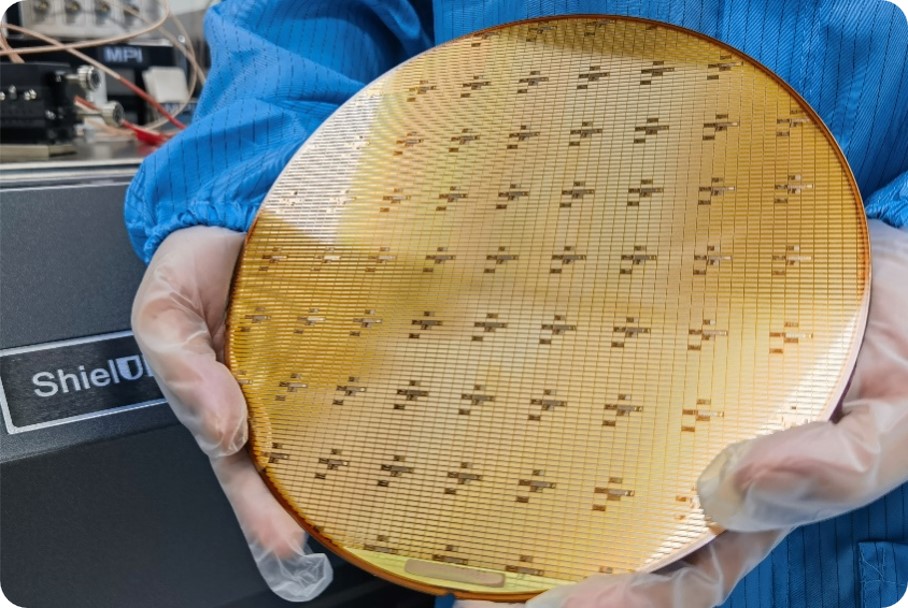
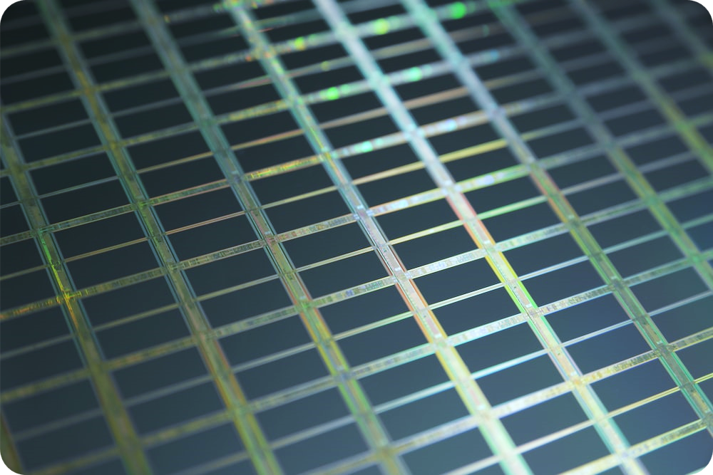
Inside the production
Industries
Processes & technical limits
| Processes | Tolerance | Max. part | Weight | Lot size | Materials |
|---|---|---|---|---|---|
| GaN/SiC power devices and driver solutionsEngineering | – | – | – | – | Gallium Nitride (GaN), Silicon Carbide (SiC) |
| Smart-GaN™ SiP (system-in-package: integrated GaN HEMT and driver IC)Engineering | – | – | – | – | Gallium Nitride (GaN) |
| Smart-Drive™ IC – driver IC for GaN, SiC, IGBTs and MOSFETsEngineering | – | – | – | – | Gallium Nitride (GaN), Silicon Carbide (SiC) |
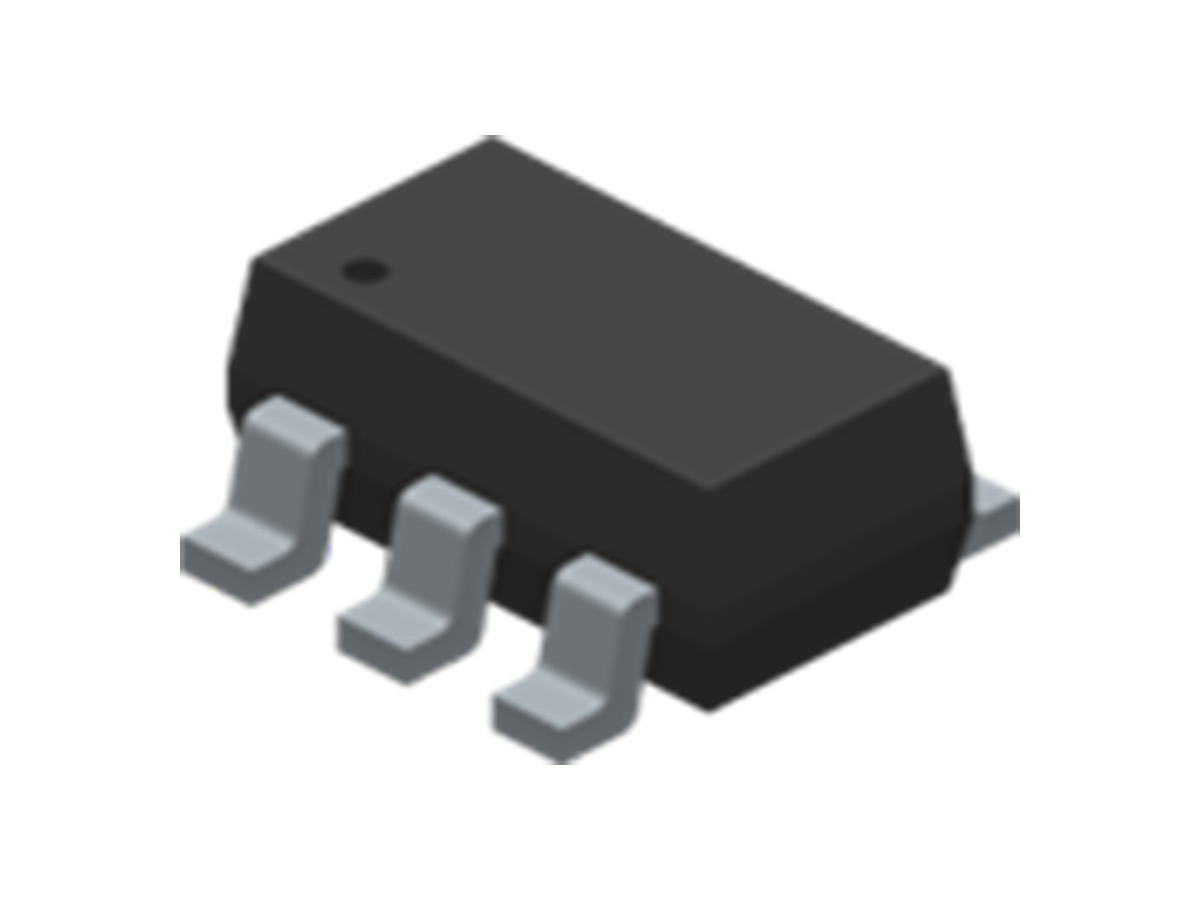
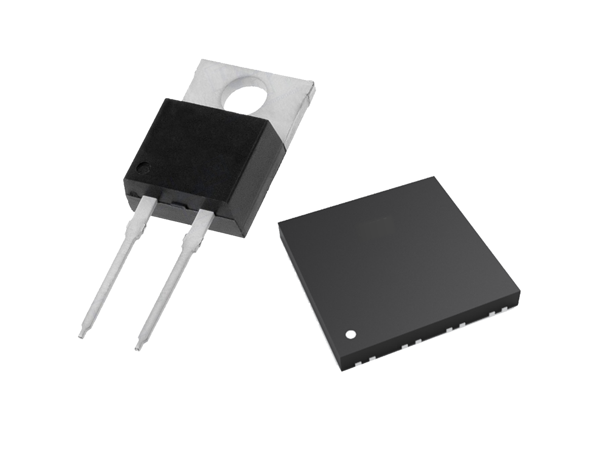
| Flash-SBD™ – GaN-on-Si Schottky barrier diode (2A – 8A)Engineering | – | – | – | – | Gallium Nitride (GaN), Silicon |
| GaN HEMTs and bare die (650V, 100 – 600mΩ Rdson)Engineering | – | – | – | – | Gallium Nitride (GaN) |
| GaN epitaxial growth (GaN-on-QST platform)Engineering | – | – | – | – | Gallium Nitride (GaN), QST substrate |
Additional services
Reference customers
History
- 2021
Founded by a team of experts from power electronics with industrial and academic backgrounds; team members (Dr. Nela, Dr. Erne) publish a research paper on multi-channel nanowire devices in Nature Electronics.
- 2022
Opening of the headquarters in Biel in the Swiss Innovation Park as the central R&D and design center.
- 2024
Participation in PCIM Europe 2024 in Nuremberg (booth 6-210).
- 2026
Selection of DB HiTek (Korea) as foundry partner for the manufacturing of E-mode GaN power devices; participation in PCIM Europe 2026 in Nuremberg; joint test series with the University of Strathclyde: GaN driver chips of the 2511U1 series operate at –196 °C in liquid nitrogen.