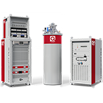
Manufactures automated materials characterization systems, cryostats and measurement technology for magnetism, low-temperature and quantum research.

Quantum Design, Inc.
San Diego, CA (World Headquarters) · Pfungstadt (Europe Headquarters) · Grimbergen · Campinas · Beijing · Shanghai · Guangzhou · Les Ulis · Budapest · Navi Mumbai · Leatherhead · Rome · Tokyo · OsakaNew on Amplifa
About Quantum Design
Quantum Design (QD) is a manufacturer of automated materials characterization systems based in San Diego, California since 1982, serving researchers in physics, chemistry, biotechnology, materials science and nanotechnology. The portfolio includes the PPMS DynaCool, MPMS 3 (SQUID magnetometer) and PPMS VersaLab measurement platforms, cryogen-free optical cryostats of the OptiCool family (7 Tesla, Vector, Flex), helium liquefiers and purifiers (NexGen160, NexGen250, ATP30), correlative AFM/SEM microscopy (FusionScope, AFSEM nano) and NV magnetometry (ProteusQ, QDM). For sample preparation, thin-film and nanofabrication systems are distributed/offered: PVD and CVD systems (nanoPVD, nanoCVD, MiniLab), vacuum annealing up to 1000 °C, reactive ion etching and floating-zone crystal growth furnaces. In addition, the Quantum Design Oxford products (low-temperature and superconducting magnet systems, dilution cryostats) are distributed. Through more than 20 own offices in Europe, Asia and the Americas, the company with over 800 employees provides local sales, technical support, installation, training and maintenance; the Europe Headquarters is located in Pfungstadt, Germany.
- Site
- San Diego, CA
- Processes
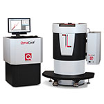
- Physical Property Measurement (PPMS DynaCool), SQUID Magnetometry (MPMS 3), Physical Property Measurement (PPMS VersaLab), Optical Spectroscopy in the Cryostat (OptiCool 7 Tesla, Vector, Flex), Helium Liquefaction and Purification (NexGen160, NexGen250, ATP30), Correlative AFM/SEM Microscopy (FusionScope), AFM Insert for SEM/FIB (AFSEM nano), Electron Diffraction (ELDICO ED-1)
- Materials
- Metals (thin film), Dielectrics, Ceramics, Organics, Graphene, Carbon Nanotubes, Physical Vapor Deposition, Chemical Vapor Deposition
- Founded
- 1982
- Employees
- 800+
- Industries
- Physics, Chemistry, Biotechnology, Materials Science, Nanotechnology, Quantum Technologies
- 01
System development and engineering
- 02
Manufacturing and assembly of measurement systems and cryostats
- 03
Installation at customers
- 04
Training and application consulting
- 05
Customer service, maintenance and repairs (including remote support)
- 06
Spare parts and consumables
Processes & Applications
Physical Vapor Deposition
Thin films of metals, oxides, nitrides, dielectrics, organics and ceramics (nanoPVD, MiniLab).
Chemical Vapor Deposition
Synthesis of graphene and carbon nanotubes up to 1100 °C, including wafer-scale (nanoCVD).
Reactive Ion Etching
Gentle, precise etching of sensitive layers such as graphene and 2D materials (nanoETCH).
Vacuum Annealing
Thermal treatment of 2D materials and wafers under controlled atmosphere up to 1000 °C (nanoANNEAL).
Floating-Zone Crystal Growth
Single crystal growth in the IR Image Furnace or Laser Furnace with 1.5 kW and 2 kW.
Locations

San Diego, CA
USWorld Headquarters, manufacturing and development
- PPMS DynaCool
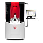
- MPMS 3
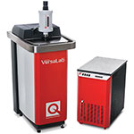
- PPMS VersaLab
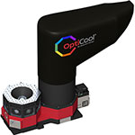
- OptiCool 7 Tesla / Vector / Flex
- NexGen160, NexGen250, ATP30
- HAC 900, HLC 4900
- FusionScope
Pfungstadt
DEEurope Headquarters; sales and support for Germany, Austria and the Middle East
Grimbergen
BEBenelux sales office
Beijing
CNSales and service office
Shanghai
CNSales and service office
Guangzhou
CNSales and service office
Singapore
SGSoutheast Asia sales and service office
Yverdon
CHSwitzerland sales and service office
Systems & Components
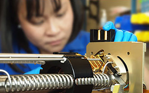
Inside the production
Industries
Processes & technical limits
| Processes | Tolerance | Max. part | Weight | Lot size | Materials |
|---|---|---|---|---|---|
| Physical Property Measurement (PPMS DynaCool)Testing | – | – | – | – | Materials characterization of solid-state samples |
| SQUID Magnetometry (MPMS 3)Testing | – | – | – | – | – |
| Physical Property Measurement (PPMS VersaLab)Testing | – | – | – | – | – |
| Optical Spectroscopy in the Cryostat (OptiCool 7 Tesla, Vector, Flex)Testing | – | – | – | – | – |
| Helium Liquefaction and Purification (NexGen160, NexGen250, ATP30)Engineering | – | – | – | – | – |
| Correlative AFM/SEM Microscopy (FusionScope)Testing | – | – | – | – | – |
| AFM Insert for SEM/FIB (AFSEM nano)Testing | – | – | – | – | – |
| Electron Diffraction (ELDICO ED-1)Testing | – | – | – | – | crystalline samples |
| Single-Crystal Orientation via Laue (s-Laue)Testing | – | – | – | – | – |
| FMR Spectroscopy (PhaseFMR / CryoFMR / ST-FMR)Testing | – | – | – | – | – |
| Magnetron Sputtering (nanoPVD-S10A)Surface | – | 4" diameter substrates | – | – | Metals, Oxides, Nitrides, Dielectrics, Organics, Ceramics |
| Thermal Evaporation (nanoPVD-T15A)Surface | – | 4" diameter substrates | – | – | Metals, Organics |
| Chemical Vapor Deposition CVD Graphene/CNT (nanoCVD-8G)Surface | – | 20 × 40 mm² substrate | – | – | Graphene, Carbon nanotubes |
| Wafer-scale CVD Graphene, optional Plasma (nanoCVD-WG/WGP)Surface | – | 3" or 4" wafers | – | – | Graphene |
| Modular Vacuum PVD Systems (MiniLab 026/060/080/090/125)Surface | – | up to 6" or 11" substrates | – | – | Metals, Dielectrics, Organics |
| Reactive Ion Etching (nanoETCH / RIE)Surface | – | – | – | – | Graphene, 2D materials |
| Vacuum Annealing up to 1000 °C (nanoANNEAL)Heat Treatment | – | – | – | – | 2D materials, Wafers |
| Floating-Zone Crystal Growth (IR Image Furnace, Laser Furnace 1.5 kW / 2 kW)Engineering | – | – | – | – | – |
| Nanofabrication (μLaser, μAligner, μCoater, μExposer)Engineering | – | – | – | – | – |
26 Anlagen & Maschinen
| Machine | Manufacturer / model | Quantity | Working area | Year built | Site |
|---|---|---|---|---|---|
| Physical Property Measurement System (PPMS DynaCool) | Quantum Design DynaCool | – | – | – | San Diego, CA, USA |
| SQUID Magnetometer | Quantum Design MPMS 3 | – | – | – | San Diego, CA, USA |
| Compact Physical Property Measurement System | Quantum Design VersaLab | – | – | – | San Diego, CA, USA |
| Cryogen-Free Optical Cryostat 7 Tesla / Vector | Quantum Design OptiCool / OptiCool Vector / OptiCool Flex | – | – | – | San Diego, CA, USA |
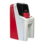
| Helium Liquefier and Purifier | Quantum Design NexGen160, NexGen250, ATP30 | – | – | – | San Diego, CA, USA |
| Helium Compressors | Quantum Design HAC 900, HLC 4900 | – | – | – | San Diego, CA, USA |
| Correlative AFM/SEM Microscopy Platform | Quantum Design FusionScope | – | – | – | San Diego, CA, USA |
| AFM Insert for SEM/FIB | AFSEM nano | – | – | – | – |
| Scanning NV Microscope | Qnami ProteusQ | – | – | – | – |
| Quantum Diamond Microscope | EuQlid QDM | – | – | – | – |
| FMR Spectrometer | NanOsc Instruments PhaseFMR / CryoFMR / ST-FMR | – | – | – | – |
| Electron Diffractometer | ELDICO Scientific ED-1 | – | – | – | – |
| Single-Crystal Orientation System (Laue) | Pulstec s-Laue | – | – | – | – |
| PCD Detectors and Imaging Cameras | ADVACAM MiniPIX, WidePIX, AdvaPIX | – | – | – | – |
| Bench-Top Charge Photometer | illumion illumionONE | – | – | – | – |
| Optical Laser Traps | Aresis TWEEZ | – | – | – | – |
| Magnetron Sputtering System (Benchtop) | Moorfield Nanotechnology nanoPVD-S10A | – | Substrates up to 4" diameter; base pressure <5×10⁻⁷ mbar | – | – |
| Thermal Evaporation System (Benchtop) | Moorfield Nanotechnology nanoPVD-T15A | – | Substrates up to 4" diameter | – | – |
| CVD Graphene Synthesis System (Benchtop) | Moorfield Nanotechnology nanoCVD-8G | – | 20 × 40 mm²; 1100 °C max. | – | – |
| Wafer-Scale CVD System | Moorfield Nanotechnology nanoCVD-WG(P) | – | 3"/4" wafers; 1100 °C; base <5×10⁻⁷ mbar | – | – |
| Modular PVD Floor System | Moorfield Nanotechnology MiniLab 026 | – | Substrates up to 6"; chamber 305 mm ID × 350 mm | – | – |
| Modular PVD Floor System | Moorfield Nanotechnology MiniLab 060 | – | Substrates up to 11"; chamber 400×400×400 mm | – | – |
| Vacuum Annealing System | Moorfield Nanotechnology nanoANNEAL | – | up to 1000 °C | – | – |
| Reactive Ion Etching System | Moorfield Nanotechnology nanoETCH | – | – | – | – |
| IR Image Furnace (2-Mirror Floating Zone) | IR Image Furnace | – | – | – | – |
| Laser Floating Zone Furnace | Laser Furnace 1.5 kW / 2 kW | – | – | – | – |
Additional services
Reference customers
History
- 1982
Quantum Design founded in San Diego, California.
- 2024
Stuart Schoenmann becomes Global CEO of Quantum Design.
- 2025
Scott Krog (CFO) and Melinda Kimbro (CHRO) join the company.
- 2026
Acquisition of Qnami (second acquisition in 2026); introduction of the Quantum Design Oxford Ultra-low-temperature cryostats.