
Develops and manufactures high-performance semiconductors and embedded solutions for automotive, industrial and connected technologies.

Renesas Electronics Corporation
New on Amplifa
About Renesas Electronics
Renesas Electronics Corporation is a publicly listed semiconductor manufacturer headquartered in Japan that develops microcontrollers, microprocessors, system-on-chips, analog ICs, power and connectivity products as well as related embedded software and development tools. The portfolio includes 32-bit MCUs (RA family with Arm Cortex-M), RL78 MCUs, RZ MPUs for HMI and edge AI as well as GaN power semiconductors for power conversion from 45 W to over 10 kW. The GaN technology is based on a vertically integrated model with in-house wafer fabrication, including epitaxial materials, device structure and packaging; in the analog domain, the PR40 process on bonded-SOI substrates is used for high-voltage precision analog applications. In addition to discrete GaN FETs, drivers and controllers, Renesas offers evaluation and prototyping boards, reference designs and AI development tools such as DRP-AI Translator and DRP-AI TVM. Target industries include automotive, industrial and factory automation, infrastructure and IoT, consumer electronics, communications infrastructure, renewable energy, robotics and healthcare. The company employs more than 21,000 people in over 30 countries.
- Processes
- Semiconductor design and embedded system solutions (MCU, MPU, SoC, analog, power, connectivity), In-house GaN wafer fabrication (vertically integrated wafer process model, epitaxial materials,, GaN power semiconductors: discrete GaN FETs (100V REXGaN®, 650V dual-side cooled 8x8mm), Hi-Rel, IC packaging (e.g. FCLGA 5×6 mm, WLCSP, STQFN, SOI substrates), PR40 process: complementary bipolar process on bonded-SOI substrates for, Embedded software and tool development (e² studio, FSP, DRP-AI Translator, DRP-AI TVM, e-AI, Reference design and system solution development (HMI, motor control, power conversion 45W–>10kW,, Evaluation board/kit development and provision (fast prototyping boards, evaluation kits,
- Materials
- Gallium nitride (GaN), Silicon (semiconductor wafer), Bonded-SOI substrate
- Employees
- 21.000+
- Industries
- Automotive, Industrial/Industrial Automation, Infrastructure & IoT, Consumer Electronics, Communications Infrastructure, Renewable Energy/Grid
- 01
Chip design (MCU, MPU, SoC, analog, power, connectivity)
- 02
In-house GaN wafer fabrication (vertically integrated process model)
- 03
IC packaging (FCLGA, WLCSP, STQFN, SOI substrates)
- 04
Embedded software and tool development
- 05
Reference design and system solution development
- 06
Evaluation board/kit development and provision
- 07
Technical support via Engineering Community
Materials & Processes
Gallium nitride (GaN)
Power semiconductors in a vertically integrated wafer process model for highly efficient, high-density power conversion from 45 W to over 10 kW.
Silicon (semiconductor wafer)
Base material for microcontrollers, microprocessors, analog ICs and power products.
Bonded-SOI substrate
Substrate of the PR40 process, a complementary bipolar process for high-voltage precision analog applications.
Products & Packages
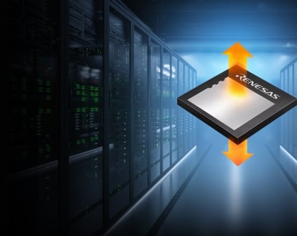
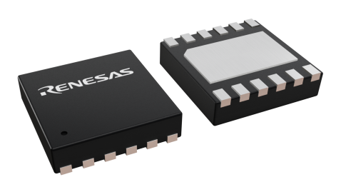
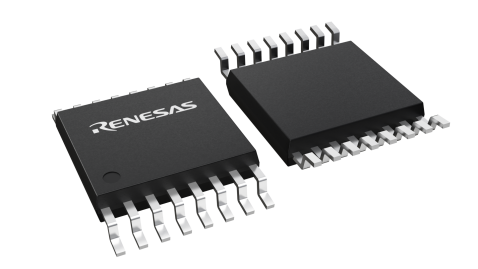
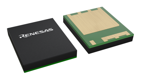
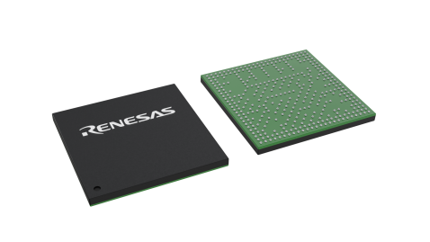
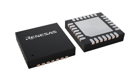
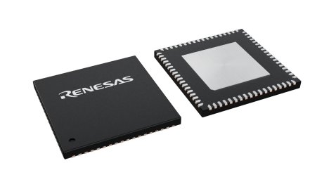
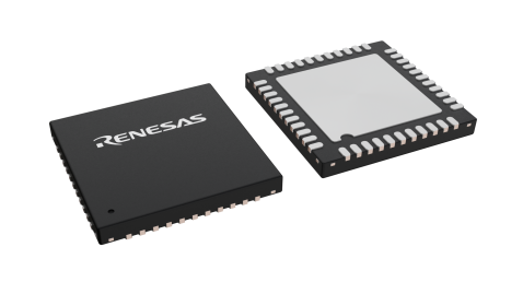
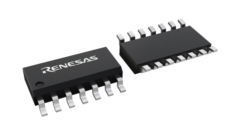
Inside the production



Industries
Processes & technical limits
| Processes | Tolerance | Max. part | Weight | Lot size | Materials |
|---|---|---|---|---|---|
| Semiconductor design and embedded system solutions (MCU, MPU, SoC, analog, power, connectivity)Engineering | – | – | – | – | Gallium nitride (GaN), Silicon |
| In-house GaN wafer fabrication (vertically integrated wafer process model, epitaxial materials,Other | – | – | – | – | Gallium nitride (GaN) |
| GaN power semiconductors: discrete GaN FETs (100V REXGaN®, 650V dual-side cooled 8x8mm), Hi-RelOther | – | – | – | – | Gallium nitride (GaN) |
| IC packaging (e.g. FCLGA 5×6 mm, WLCSP, STQFN, SOI substrates)Other | – | – | – | – | Gallium nitride (GaN), Silicon |
| PR40 process: complementary bipolar process on bonded-SOI substrates forOther | – | – | – | – | Silicon, SOI substrate |
| Embedded software and tool development (e² studio, FSP, DRP-AI Translator, DRP-AI TVM, e-AIEngineering | – | – | – | – | – |
| Reference design and system solution development (HMI, motor control, power conversion 45W–>10kW,Engineering | – | – | – | – | – |
| Evaluation board/kit development and provision (fast prototyping boards, evaluation kits,Engineering | – | – | – | – | – |
Additional services
History
- 2019
Collaboration with Xilinx on Versal ACAP reference designs; introduction of the 32-bit RA MCU family (Arm Cortex-M) and the Bluetooth 5 MCU RX23W.
- 2020
Introduction of the 32-bit RA MCU family (Arm Cortex-M) for IoT applications.
- 2023
Renesas released its first Wi-Fi development kit with support for the Matter protocol.
- 2024
Japan's first lunar lander SLIM landed with radiation-hardened ICs from Renesas (Intersil brand) on board.