
Develops and manufactures UHV instruments for electron spectroscopy, scanning probe microscopy and thin-film deposition
Scienta Omicron GmbH
Uppsala (SE) · Taunusstein (DE) · Denver, CO (US) · Beijing (CN) · Seoul (KR)New on Amplifa
About Scienta Omicron
Scienta Omicron is a manufacturer of high-technology instruments for surface physics and nanotechnology. At its technology centers in Uppsala (Sweden) and Taunusstein (Germany), the company develops and produces systems for electron spectroscopy (XPS/ESCA, ARPES, HAXPES, APXPS), scanning probe microscopy (STM, AFM) and thin-film deposition (molecular beam epitaxy, thermal evaporation, sputtering), all for use under ultrahigh vacuum (UHV). In addition to individual components, custom UHV clusters are offered as Materials Innovation Platforms (MIP), based on a platform strategy with more than 85 surface analysis and deposition techniques and over 1,000 delivered UHV systems. Customers include research institutions and industry, particularly in battery and materials research, quantum technologies, electronics, the solar industry and sensor technology. Sales and service are provided worldwide through four regional hubs in the USA, China, Japan and Germany, as well as partners in South Korea, Singapore, Taiwan, Australia and India.
- Site
- Taunusstein
- Processes
- Electron spectroscopy (XPS, ESCA), Photoelectron spectroscopy (PES, ARPES), HAXPES (hard X-ray photoelectron spectroscopy, as a service: ACCESS-HAXPES), APPES / APXPS (ambient-pressure photoelectron spectroscopy), Scanning probe microscopy (SPM): STM, AFM, Molecular beam epitaxy (MBE) / thin-film deposition, Thermal evaporation and sputtering (thin-film deposition), Scanning electron microscopy (SEM, UHV Gemini)
- Materials
- Tantalum nitride (Ta₃N₅), NiOx (nickel oxide), Silicon (Si(111) 7x7, silicon surface), Gold (Au(111) surface), Niobium diselenide (NbSe2), Sodium chloride (NaCl(100)), Tantalum (Ta pins, Ta foil in VUV5k source), Photoelectron spectroscopy (XPS, ARPES, HAXPES, APPES)
- Industries
- Surface physics and nanotechnology, Materials research (batteries, quantum technologies, electronics, solar, Research institutions and universities, Surface physics and nanotechnology research, Science/research institutions
- 01
System design and engineering
- 02
Manufacture and assembly of UHV components
- 03
Integration of analysis and deposition modules
- 04
Installation at the customer's site
- 05
Service, maintenance and upgrades
- 06
Training and consulting
Technologies and Processes
Photoelectron spectroscopy (XPS, ARPES, HAXPES, APPES)
Measures chemical and electronic states in materials, from surfaces to the bulk.
Scanning probe microscopy (STM, AFM)
Images the physical structure of surfaces down to the atomic level.
Molecular beam epitaxy / thin-film deposition
Builds up material samples through epitaxial growth under UHV conditions.
Ultrahigh vacuum system technology
Platform base (CREATE, LTL, RDC, MISTRAL) for custom multi-technique systems.
Locations
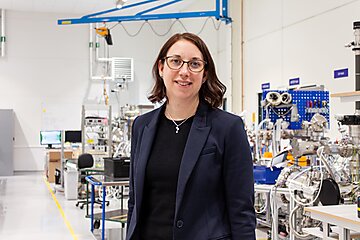
Uppsala
SEHeadquarters and technology center (development and production)
- ARPES analysis systems (R4000, DA30-L, DA20)
- SPM systems
- MBE systems
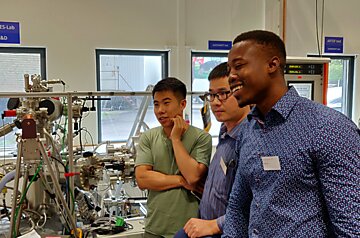
Taunusstein
DETechnology center (development and production); sales and service Europe/rest of world
- UHV system manufacturing
- Application laboratory
- MISTRAL control systems
Denver, CO
USRegional hub for sales and service in the Americas
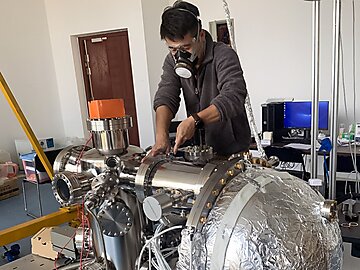
Beijing
CNRegional hub for sales and service in China
Seoul
KRSales and service in South Korea
Instruments and Components

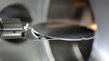
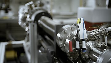
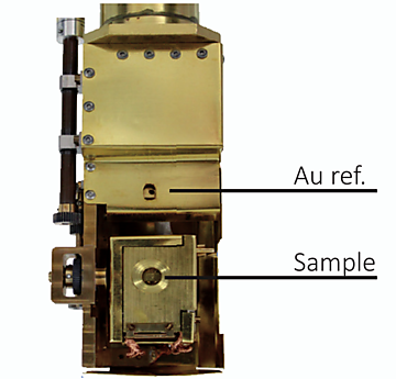
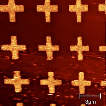
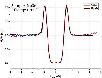
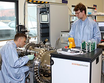
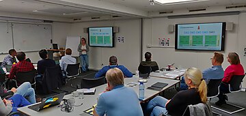
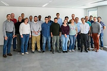
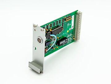
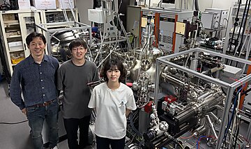
Inside the production
Industries
Processes & technical limits
| Processes | Tolerance | Max. part | Weight | Lot size | Materials |
|---|---|---|---|---|---|
| Electron spectroscopy (XPS, ESCA)Testing | – | – | – | – | – |
| Photoelectron spectroscopy (PES, ARPES)Testing | – | – | – | – | – |
| HAXPES (hard X-ray photoelectron spectroscopy, as a service: ACCESS-HAXPES)Testing | – | – | – | – | – |
| APPES / APXPS (ambient-pressure photoelectron spectroscopy)Testing | – | – | – | – | – |
| Scanning probe microscopy (SPM): STM, AFMTesting | – | – | – | – | – |
| Molecular beam epitaxy (MBE) / thin-film depositionAdditive | – | – | – | – | – |
| Thermal evaporation and sputtering (thin-film deposition)Additive | – | – | – | – | – |
| Scanning electron microscopy (SEM, UHV Gemini)Testing | – | – | – | – | – |
| Auger electron spectroscopy (AES/NanoSAM)Testing | – | – | – | – | – |
| LEED (low-energy electron diffraction)Testing | – | – | – | – | – |
| Sputtering / ion etching for sample cleaning and depth profiling (FDG15/FDG150 ion source)Surface | – | – | – | – | – |
| Lithography in UHV-SPM (large-scale lithography, e.g. qubit structures)Engineering | – | – | – | – | Silicon, Gold |
| UHV sample manipulation (open/closed cycle sample manipulators, <3.5 K to RT)Engineering | – | – | – | – | – |
| Materials innovation platforms (MIP) - UHV clusters with growth and in-situ characterizationEngineering | – | – | – | – | – |
| UHV system design and custom system solutions (CREATE platform, >85 surface analysis andEngineering | – | – | – | – | – |
| System service, maintenance, upgrades, training, consultingEngineering | – | – | – | – | – |
22 Anlagen & Maschinen
| Machine | Manufacturer / model | Quantity | Working area | Year built | Site |
|---|---|---|---|---|---|
| LT STM (low-temperature scanning tunneling microscope) | Scienta Omicron LT STM | – | Extended Range Scanner: >10x10x0.5 µm³ at 77 K; >4x4x0.3 µm³ at 5 K | – | – |
| SPM (scanning probe microscope) | Scienta Omicron POLAR | – | – | – | – |
| SPM (scanning probe microscope, closed cycle, 9 K) | Scienta Omicron INFINITY | – | – | – | – |
| SPM (scanning probe microscope) | Scienta Omicron STREAM | – | – | – | – |
| UHV-SEM (scanning electron microscope) | Scienta Omicron UHV Gemini | – | Scan parameters 10 ns to 500 ms | – | – |
| Hemispherical analyzer (photoelectron spectroscopy) | Scienta Omicron DA30-L | – | – | – | – |
| Hemispherical analyzer / ARPES lab | Scienta Omicron DA20 | – | – | – | – |
| ARPES analysis system | Scienta Omicron R4000 | – | – | – | – |
| Analyzer systems | Scienta Omicron EW4000, HiPP-3, DFS30 | – | – | – | – |
| Ion sputter source | Scienta Omicron FDG15 | – | Spot size variable from 300 µm to 10 mm | – | – |
| Fine-focus ion source | Scienta Omicron FDG 150 | – | – | – | – |
| Materials innovation platform (UHV cluster) | Scienta Omicron MIP | – | – | – | – |
| UHV platform / modular system | Scienta Omicron CREATE Platform | – | – | – | – |
| Linear transfer line (UHV sample handling) | Scienta Omicron LTL | – | – | – | – |
| Radial distribution chamber (rotatable transfer arm, up to 4" wafers) | Scienta Omicron RDC | – | up to 4" wafers | – | – |
| UHV vacuum control system | Scienta Omicron MISTRAL | – | – | – | – |
| UHV transport suitcase (up to 6 sample holders) | Scienta Omicron UHV Suitcase | – | – | – | – |
| Vacuum UV source | Scienta Omicron VUV5k | – | – | – | – |
| MBE system with integrated analysis | Omicron | – | – | 2000 | – |
| Photoelectron microscopy system | Scienta Omicron NanoESCA | – | – | 2007 | – |
| Low-temperature nanoprobe | Scienta Omicron LT Nanoprobe | – | – | 2013 | – |
| Variable-temperature STM (4 to over 1000 K) | Omicron VT STM | – | – | 1996 | – |
Additional services
Reference customers
History
- 1983
Founding of Scienta, originating from the 1981 Nobel Prize awarded to Kai Siegbahn (ESCA/XPS)
- 1984
Founding of Omicron (Omicron Vakuumphysik GmbH) by Norbert Nold and Ernst Lang
- 1987
First commercial UHV-STM (STM 1)
- 1996
VT STM receives the R&D 100 Award
- 1999
Omicron recognized as a "Hidden Champion"
- 2000
First MBE system with integrated analysis capability
- 2007
NanoESCA system receives the R&D 100 Award
- 2011
Omicron becomes part of Oxford Instruments plc
- 2013
LT Nanoprobe system receives the R&D 100 Award
- 2015
Merger of VG Scienta and Omicron NanoTechnology to form Scienta Omicron