
Technology representation and sourcing platform for semiconductor equipment, metrology, inspection and spare parts in Europe
Seteco
FreiamtNew on Amplifa
About Seteco
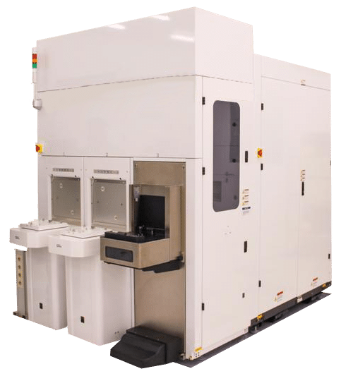
Seteco was founded in 2004 in Freiamt (Black Forest) and, as a sole proprietorship, operates exclusively in the semiconductor industry. The company connects providers of semiconductor technology with European fabs, OEMs and research institutes through technology representation, technical sales, spare parts sourcing and equipment solutions. It officially represents GTI (METREX) with remanufactured CD-SEM, DR-SEM and darkfield inspection systems based on Applied Materials platforms, Comet with 2D and 3D X-ray/CT inspection systems, and CMTec with used and refurbished wire and die bonders along with pull and shear testers. In addition, Seteco operates its own sourcing platform with over 1000 spare parts in stock for platforms from August/Rudolph Technologies (ONTO), KLA Tencor, AMAT and Comet Yxlon, and procures hard-to-find, obsolete components through a European and worldwide partner network. Complementing this, the company offers software solutions for data analysis, defect mapping and recipe management as well as technical consulting for market entry in Europe. Customers come from the semiconductor industry, electronics, automotive, power electronics, MEMS and sensor technology.
- Site
- Freiamt
- Processes
- CD-SEM Measurement (Critical Dimension Metrology), Defect Review DR-SEM, Darkfield Patterned Wafer Inspection (defects from 70 nm), Wafer and Mask Inspection (remanufactured platforms), 2D & 3D X-Ray / CT Inspection (non-destructive testing), Wire Bonding (refurbished equipment), Die Bonding (refurbished equipment), Pull & Shear Testing (bond tests)
- Materials
- SiC (Silicon Carbide), GaAs (Gallium Arsenide), InP (Indium Phosphide), Glass (Substrates), III-V Semiconductors
- Founded
- 2004
- Industries
- Semiconductor Industry, Fabs, OEMs, Advanced Packaging, Electronics, Automotive
- 01
Technology Representation & Business Development
- 02
Technical Sales
- 03
Spare Parts Sourcing (warehouse, partner network, procurement)
- 04
Refurbished Equipment & Inspection Systems
- 05
Service, Training & Applications Support
- 06
Software & Technical Consulting
Materials & Applications
SiC (Silicon Carbide)
Substrate material measured via CD-SEM metrology on Applied Materials platforms.
GaAs (Gallium Arsenide)
Compound semiconductor substrate suitable for metrology and defect review.
InP (Indium Phosphide)
III-V substrate covered by GTI metrology systems.
III-V Semiconductors
Material class for compound substrates used in CD-SEM and DR-SEM applications.
Glass (Substrates)
Glass substrates processed as part of critical dimension metrology.
Locations
Freiamt
DEHeadquarters, Sales & Representation
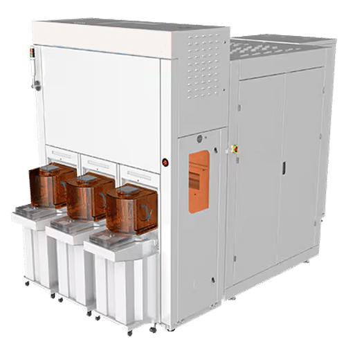
- CD-SEM / DR-SEM metrology systems (GTI/METREX, VERITY NextGEN, SEMVision NextGEN)
- Darkfield inspection systems (Compass, Complus, WF)
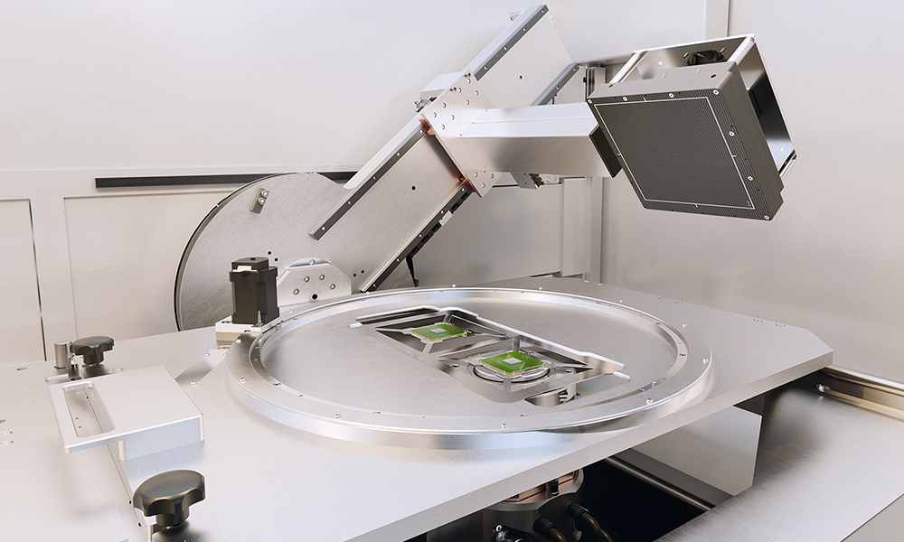
- 2D & 3D X-ray/CT inspection systems (Comet CA20, Cheetah EVO, FF series)
- Wire Bonder / Die Bonder (refurbished, CMTec)
- Pull & Shear Tester (CMTec)
- Wafer and reticle inspection systems (remanufactured, RTEX)
- Spare parts warehouse (1000+ parts)
Spare Parts & Equipment
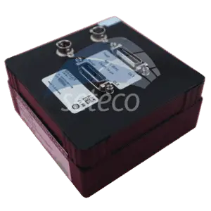
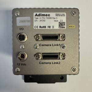
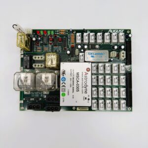
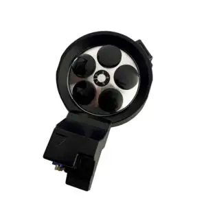
Inside the production
Industries
Processes & technical limits
| Processes | Tolerance | Max. part | Weight | Lot size | Materials |
|---|---|---|---|---|---|
| CD-SEM Measurement (Critical Dimension Metrology)Testing | – | – | – | – | SiC, GaAs, InP, Glass, III-V Semiconductors, Silicon Wafers |
| Defect Review DR-SEMTesting | – | – | – | – | SiC, GaAs, InP, III-V Semiconductors |
| Darkfield Patterned Wafer Inspection (defects from 70 nm)Testing | – | – | – | – | Silicon Wafers |
| Wafer and Mask Inspection (remanufactured platforms)Testing | – | – | – | – | – |
| 2D & 3D X-Ray / CT Inspection (non-destructive testing)Testing | – | – | – | – | – |
| Wire Bonding (refurbished equipment)Joining | – | – | – | – | – |
| Die Bonding (refurbished equipment)Assembly | – | – | – | – | – |
| Pull & Shear Testing (bond tests)Testing | – | – | – | – | – |
| Spare Parts Sourcing & RefurbishmentEngineering | – | – | – | – | – |
| Technical Consulting / Market Development / Process ConsultingEngineering | – | – | – | – | – |
| Software Solutions (Data Analysis, Defect Mapping, Recipe Management)Engineering | – | – | – | – | – |
7 Anlagen & Maschinen
| Machine | Manufacturer / model | Quantity | Working area | Year built | Site |
|---|---|---|---|---|---|
| CD-SEM (Critical Dimension SEM) | GTI (METREX, based on Applied Materials) VeritySEM / VERITY NextGEN | – | Wafers 6"/150mm, 8"/200mm, 12"/300mm; wafer thickness up to 2mm | – | Freiamt, Germany (sales/representation) |
| DR-SEM Defect Review SEM (with/without FIB) | GTI (METREX, based on Applied Materials) SEMSVision NextGEN | – | Wafers 150-300mm; wafer thickness up to 2mm | – | Freiamt, Germany (sales/representation) |
| Darkfield Inspection System | GTI (METREX) Compass / Complus / WF | – | Patterned wafers, defects from 70 nm | – | Freiamt, Germany (sales/representation) |
| 2D & 3D X-Ray / CT Inspection Systems | Comet CA20, Cheetah EVO, FF series CT | – | – | – | Freiamt, Germany (sales/representation) |
| Wire Bonder / Die Bonder (used/refurbished) | CMTec AG | – | – | – | Freiamt, Germany (sales) |
| Pull & Shear Tester | CMTec AG | – | – | – | Freiamt, Germany (sales) |
| Wafer and Reticle Inspection Systems (remanufactured) | RTEX | – | – | – | Freiamt, Germany (sales/representation) |
Additional services
History
- 2004
Founded in Freiamt with a specialized semiconductor focus.
- 2012
GTI (Green Technology Investments) offers inspection and metrology solutions based on Applied Materials platforms.
- 2020er
Over 20 years of presence in semiconductor sales & service, official representation of three technology partners (GTI, Comet, CMTec).