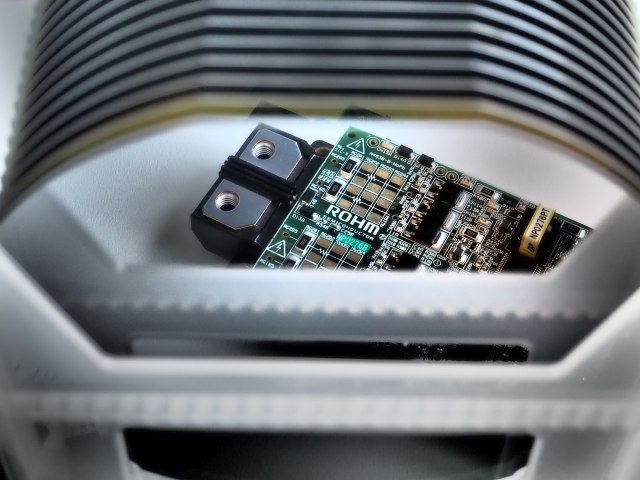
Manufacture of single-crystal silicon carbide substrates and wafers for the semiconductor industry.

SiCrystal GmbH
NurembergNew on Amplifa
About SiCrystal
SiCrystal GmbH, based in Nuremberg, produces and supplies high-quality single-crystal silicon carbide substrates (SiC wafers), which serve as the basis for manufacturing innovative, energy-efficient electronic components. Single-crystal silicon carbide is a transparent, extremely hard and temperature-insensitive semiconductor material with exceptional electrical properties. The typical wafers have a diameter of 150 millimeters and a thickness of 350 micrometers and must meet a specification defined in detail by the customer. The company covers all manufacturing steps: in-house production of the key raw materials, high-temperature crystal growth from the gas phase, precise mechanical machining of crystals and wafers, as well as semiconductor-compatible cleaning and final quality control in the cleanroom. In addition to standard-quality wafers for industrial further processing at leading semiconductor groups, Engineering-Grade wafers for research and development are offered. SiCrystal is a company of the Japanese Rohm Group and supplies key customers worldwide in the fields of the semiconductor industry, industry, and research and development.
- Site
- Nuremberg
- Processes
- High-temperature crystal growth from the gas phase (SiC crystal growth), Precise mechanical machining of crystals and wafers, Semiconductor-compatible cleaning, Final quality control in the cleanroom, In-house production of the key raw materials for crystals
- Materials
- Single-crystal silicon carbide (SiC substrates/wafers), Single-crystal silicon carbide, High-temperature crystal growth from the gas phase, Precise mechanical machining
- Certificates
- ISO 9001, ISO 14001, ISO 45001, ISO 50001
- Industries
- Semiconductor industry, Industry, Research and development
- 01
In-house production of the key raw materials for crystals
- 02
High-temperature crystal growth from the gas phase
- 03
Precise mechanical machining of crystals and wafers
- 04
Semiconductor-compatible cleaning
- 05
Final quality control in the cleanroom
Materials and Processes
Single-crystal silicon carbide
Transparent, extremely hard and temperature-insensitive semiconductor material for energy-efficient electronic components.
High-temperature crystal growth from the gas phase
Process for growing single-crystal silicon carbide crystals from in-house produced raw materials.
Precise mechanical machining
Machining of crystals and wafers with high precision up to customer specification.
Locations
Nuremberg
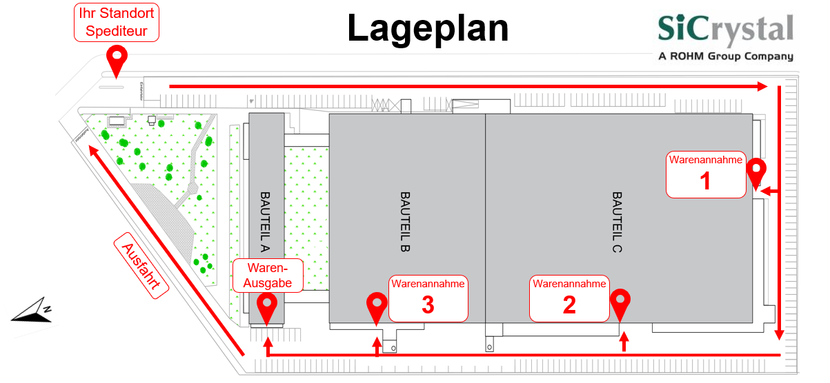
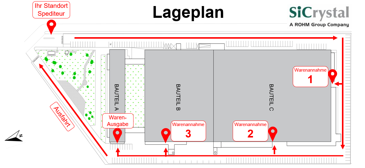
DEHeadquarters with production, goods receiving and sales
- Materials
- Single-crystal silicon carbide
- Buildings A, B & C
- Cleanroom
Products
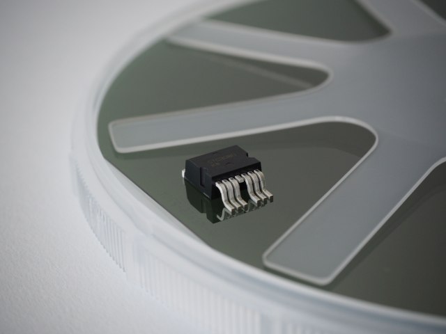
Inside the production
Industries
Processes & technical limits
| Processes | Tolerance | Max. part | Weight | Lot size | Materials |
|---|---|---|---|---|---|
| High-temperature crystal growth from the gas phase (SiC crystal growth)Casting | – | – | – | – | Single-crystal silicon carbide |
| Precise mechanical machining of crystals and wafersMachining | – | – | – | – | Single-crystal silicon carbide |
| Semiconductor-compatible cleaningSurface | – | – | – | – | Single-crystal silicon carbide |
| Final quality control in the cleanroomTesting | – | – | – | – | Single-crystal silicon carbide |
| In-house production of the key raw materials for crystalsEngineering | – | – | – | – | Single-crystal silicon carbide |
Quality and Certifications
Every process step is based on advanced methods within a continuous improvement process; the final quality control takes place in the cleanroom. The quality management system meets the requirements of the standards ISO 9001, ISO 50001, ISO 14001 and ISO 45001.
| Evidence | Nuremberg |
|---|---|
| ISO 9001 | |
| ISO 14001 | |
| ISO 45001 | |
| ISO 50001 |
History
- unbekannt
No documented historical events from the sources