
Development and manufacture of vacuum coating systems and processes for high-precision thin films and optical coatings.

SOLAYER GmbH
Karlstein am Main · Kesselsdorf near Dresden · Shanghai · Singapore · Zhunan · Taichung · Hsinchu · TainanNew on Amplifa
About SOLAYER
SOLAYER GmbH is an internationally active high-tech company in surface technology, founded in Dresden in 2007 and headquartered in Karlstein am Main. The company develops and manufactures customer-specific vacuum coating systems, including the ultra-high-precision sputtering system AVIOR M-300, the AVIOR S-100, the modular ALASCO O-200, and the ALIOTH inline platform for series production. The process portfolio covers MF, DC, DC-pulsed and RF magnetron sputtering, PECVD, thermal evaporation, ALD, IBAD, ion beam etching, RIE, PIII and Flash Lamp Annealing. Deposited functional and optical layers include ITO, AZO, IGZO, SiO2, Ta2O5, TiO2, SiNx, TiN and metals on substrates of silicon, glass (including thin glass from 0.2 mm), polymer and metal foil. Target industries include photonics, precision optics, semiconductors, displays, photovoltaics, sensors/3D sensing/LiDAR, automotive and life sciences. In addition to systems, SOLAYER offers thin-film stack simulation, material qualification, contract coating, thin-film metrology services, retrofits and spare parts supply. Locations include two Technology Centers in Karlstein and Kesselsdorf near Dresden as well as sales offices in Shanghai, Singapore and Taiwan; since 2020 AMEC (Shanghai) has been a strategic investor.
- Site
- Karlstein
- Processes
- High-precision thin-film coating / vacuum coating (thin-film deposition), MF, DC, DC-pulsed and RF magnetron sputtering, PECVD (plasma-enhanced chemical vapor deposition), Thermal evaporation, ALD (atomic layer deposition), IBAD (ion beam assisted deposition), IBE (ion beam etching) / ion milling, RIE (reactive ion etching)
- Materials
- ITO, AZO, IGZO, ZnO:X / iZnO, ZinxSnyOz, Silicon dioxide, Aluminium oxide, Tantalum pentoxide
- Founded
- 2007
- Industries
- Photonics, Precision optics, Optical filters, Semiconductors/organic semiconductors, Display, Photovoltaics
- 01
Process specification and feasibility assessment
- 02
Thin-film stack simulation and modeling
- 03
System design (mechanical and electrical engineering)
- 04
System fabrication and assembly
- 05
Material qualification and process implementation
- 06
Customer acceptance test (Qualification & Testing)
- 07
Onsite/remote support, maintenance, spare parts, up-scaling
Locations
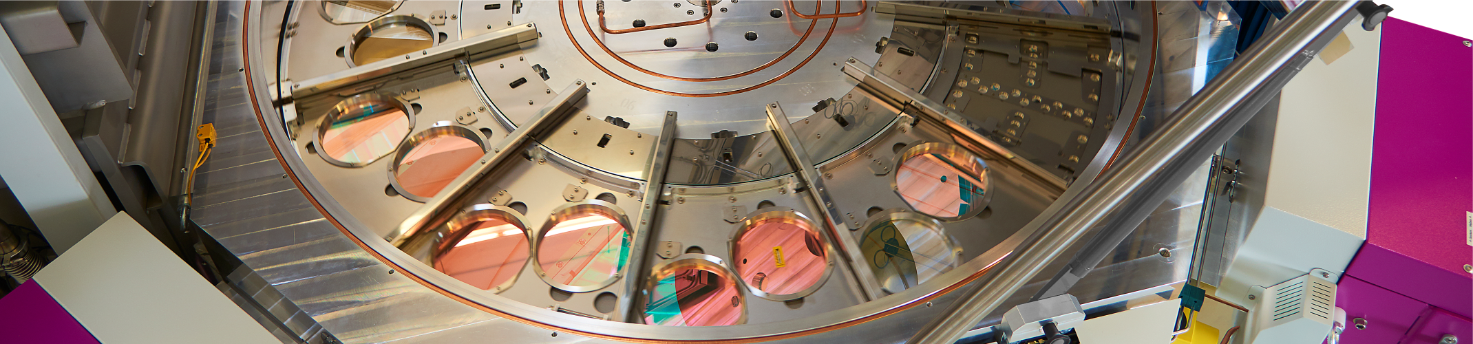
Karlstein
DEHeadquarters & Technology Center 2 – development and engineering of vacuum coating systems
- Materials
- Aluminium, copper, titanium, brass, stainless steel, plastics
- AVIOR M-300
- AVIOR S-100
- ALASCO O-200
- ALIOTH
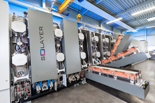
- Vertical inline coating system (PVD/PECVD)
- Horizontal inline coating system (sputtering, PECVD, ALD, FLA)
Kesselsdorf near Dresden
DETechnology Center 1 – research and development of filter technologies
Shanghai
CNSales office (AMEC China)
Singapore
SGSales office (AMEC Singapore)
Zhunan
TWSales office (AMEC Taiwan)
Taichung
TWSales office
Hsinchu
TWSales office
Tainan
TWSales office
Products & Systems
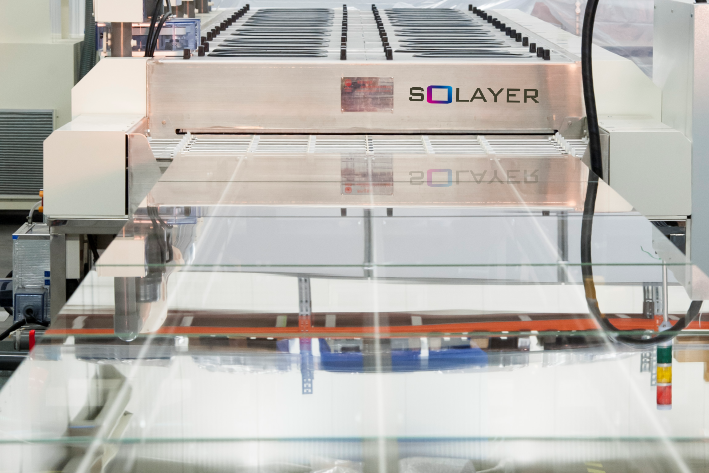
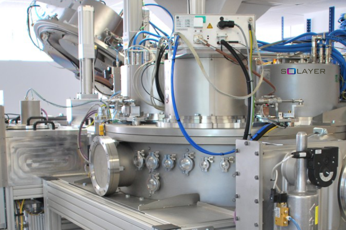
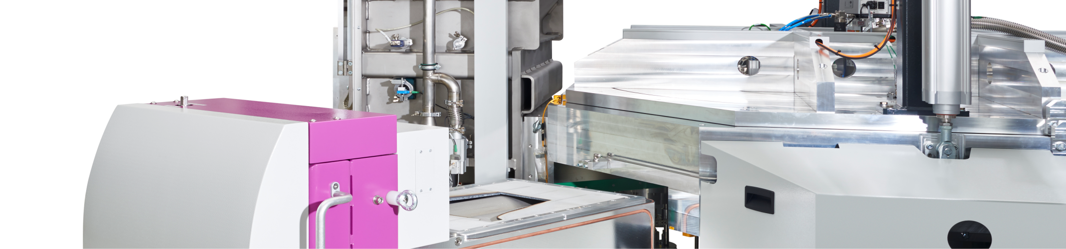
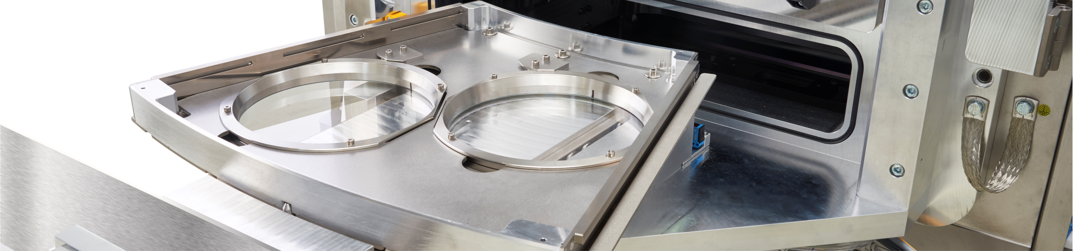
Inside the production
Industries
Processes & technical limits
| Processes | Tolerance | Max. part | Weight | Lot size | Materials |
|---|---|---|---|---|---|
| High-precision thin-film coating / vacuum coating (thin-film deposition)Surface | – | – | – | – | – |
| MF, DC, DC-pulsed and RF magnetron sputteringSurface | – | – | – | – | – |
| PECVD (plasma-enhanced chemical vapor deposition)Surface | – | – | – | – | SiO2, SiOxNy, TiOxNy, AlOxNy, SiNx |
| Thermal evaporationSurface | – | – | – | – | Mo, Cr, Al, Ag, Au, Cu, W, Ti, Ni, ZnTe, SiO2, Ta2O5, TiO2, TiN |
| ALD (atomic layer deposition)Surface | – | – | – | – | Al2O3, SiO2, TiO2, AlN, SiNx |
| IBAD (ion beam assisted deposition)Surface | – | – | – | – | Mo, Cr, Al, Ag, Au, Cu, W, Ti, Ni, SiO2, Ta2O5, TiO2, TiN, AlN, DLC, SiC |
| IBE (ion beam etching) / ion millingSurface | – | – | – | – | Si wafer, glass, metal foil, DLC, SiC |
| RIE (reactive ion etching)Surface | – | – | – | – | Si wafer, glass, DLC, SiC, AlC, SiCxOyNz |
| PIII (plasma immersion ion implantation)Surface | – | – | – | – | metal foil, glass, DLC, SiC |
| Flash Lamp Annealing (FLA) – rapid thermal treatment (RTP) of samplesHeat treatment | – | – | – | – | Si wafer, glass, SiNx, TiN |
| Surface treatment – cleaning, etching, ion implantationSurface | – | – | – | – | Si wafer, glass, polymer, metal foil |
| Optical coating (anti-reflective, filter, mirror, TCO and metal layers by sputtering)Surface | – | – | – | – | SiO2, Al2O3, Ta2O5, Nb2O5, TiO2, ZrO2, HfO2, ZnO, WO3, ITO, AZO, Ag, Au, Al, SiNx, TiOxNy |
| Thin-film metrology and characterization services in the analysis laboratoryTesting | – | – | – | – | – |
| Thin-film stack simulation and modeling (optical layer properties)Engineering | – | – | – | – | – |
| Design of customized ALD reactor tooling; mechanical & electrical system designEngineering | – | – | – | – | – |
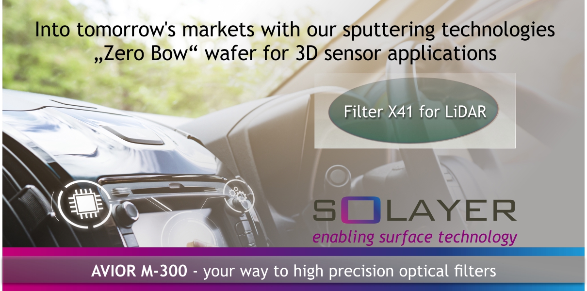
| Manufacture of NIR bandpass filters (X41) on thin glass using 'zero bow' technologySurface | – | 200 mm substrate diameter × substrate thickness < 200 µm | – | – | Si:H (hydrogenated silicon), SiO2, thin glass |
| Custom vacuum automation (substrate transport, cassette operation, cluster systems 2–8Assembly | – | – | – | – | – |
6 Anlagen & Maschinen
| Machine | Manufacturer / model | Quantity | Working area | Year built | Site |
|---|---|---|---|---|---|
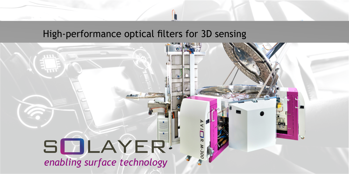
| Ultra-high-precision sputtering system (high-end production system, optical coating) | SOLAYER AVIOR M-300 | – | Universal loading for substrate sizes 12 x 300 mm, 24 x 200 mm or 48 x 150 mm; 'zero bow' process | – | Karlstein/Kesselsdorf, Germany |
| Optical sputtering system (plug & coat, small batches / market entry) | SOLAYER AVIOR S-100 | – | – | – | Karlstein/Kesselsdorf, Germany |
| Modular optical coating system (R&D and production, with PIII and FLA modules and | SOLAYER ALASCO O-200 | – | – | – | Karlstein/Kesselsdorf, Germany |
| Versatile inline coating system (dielectric, metal-dielectric and | SOLAYER ALIOTH | – | – | – | Karlstein/Kesselsdorf, Germany |
| Vertical inline coating system (PVD and PECVD module platform, continuous | SOLAYER | – | – | – | Karlstein/Kesselsdorf, Germany |
| Horizontal inline coating system (sputtering, PECVD, ALD, FLA; cleaning, etching, deposition, | SOLAYER | – | – | – | Karlstein/Kesselsdorf, Germany |
Additional services
History
- 2007
Founded in Dresden – Silicon Saxony
- 2013–2015
Establishment of representative offices in the USA, China, Taiwan, Japan, Korea and India
- 2016
Acquisition of DTF – Dresden Thin Film Technology GmbH; opening of the new Technology Center in Karlstein
- 2020
AMEC (Shanghai) becomes strategic investor; membership in EPIC; presentation of the zero-bow wafer technology for NIR bandpass filters (X41)
- 2021
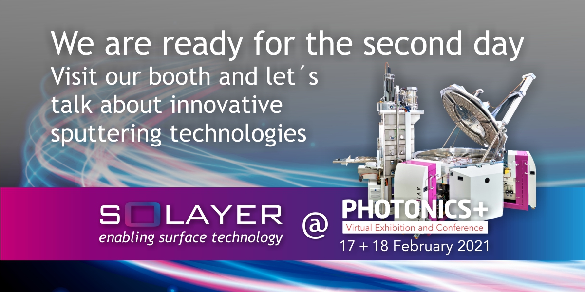
Presence at the virtual Photonics+ trade fair