Manufacturing and assembly of complex electronic assemblies: EMS, subcontracting and thick-film hybrid technology on ceramic substrates.

Spree Hybrid & Kommunikationstechnik GmbH
BerlinNew on Amplifa
About SHK
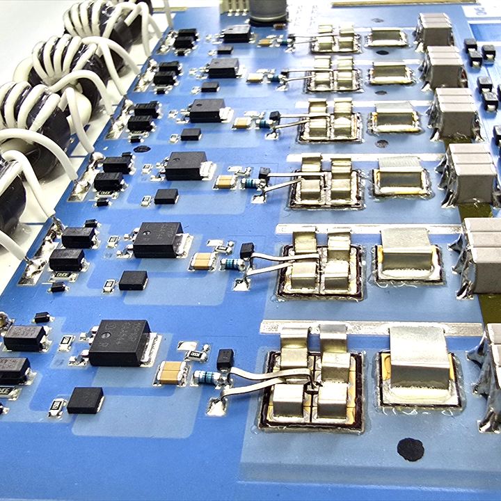
Spree Hybrid & Kommunikationstechnik GmbH (SHK) is an EMS provider in Berlin that has been manufacturing and assembling electronic assemblies since 1991. Its range of services covers full-service EMS with procurement, subcontracting with customer-supplied materials, and a specialization in custom thick-film hybrid technology: conductor tracks and resistors are applied by screen printing onto ceramic substrates, fired at around 800 °C and laser-trimmed to tolerances better than 0.1%. The assembly and interconnection technology ranges from SMD placement (fine-pitch up to BGA/µBGA) and THD insertion to selective, wave and nitrogen wave soldering; hybrid modules are suitable for high-voltage applications up to 30 kV. An in-house fixture manufacturing shop with CNC milling and 3D printing produces workpiece carriers, soldering frames and test fixtures. Customers include companies from medical technology and the automotive industry; production runs in 3-shift operation for projects worldwide.
- Site
- Berlin
- Processes
- EMS (Electronics Manufacturing Services) - electronic assembly manufacturing and assembly, SMD placement (Surface Mount Device), Reflow soldering in air or under nitrogen, THD placement (Through-Hole Device) with light-controlled placement tables, Selective soldering, Wave soldering (nitrogen wave soldering), Dip soldering, Hand soldering & rework at microscope workstations
- Materials
- Ceramic substrate, Printed circuit board (PCB), Solder paste, Thick-film pastes (conductor-track and resistor pastes), Printed circuit board (FR4)
- Certificates
- DIN EN ISO 9001:2015, ISO 9001
- Founded
- 1991
- Industries
- Medical technology, Automotive industry
- 01
Technology consulting
- 02
Material purchasing/procurement
- 03
Data review & DFM/DFT
- 04
Stencil printing
- 05
SMD/THD placement
- 06
Soldering (reflow, selective, wave)
- 07
Hybrid technology (screen printing, firing, laser trimming)
- 08
AOI & functional testing
- 09
Laser marking
- 10
Series production
Materials & Processes
Ceramic substrate
Base material of thick-film hybrid technology for high temperatures, miniaturization and high voltage up to 30 kV.
Printed circuit board (FR4)
Basis of SMD and THD assembly manufacturing from the smallest chip packages to large ICs and connectors.
Thick-film pastes (conductor-track and resistor pastes)
Applied by screen printing and fired at approx. 800 °C; resistors are laser-trimmed to better than 0.1%.
Solder paste
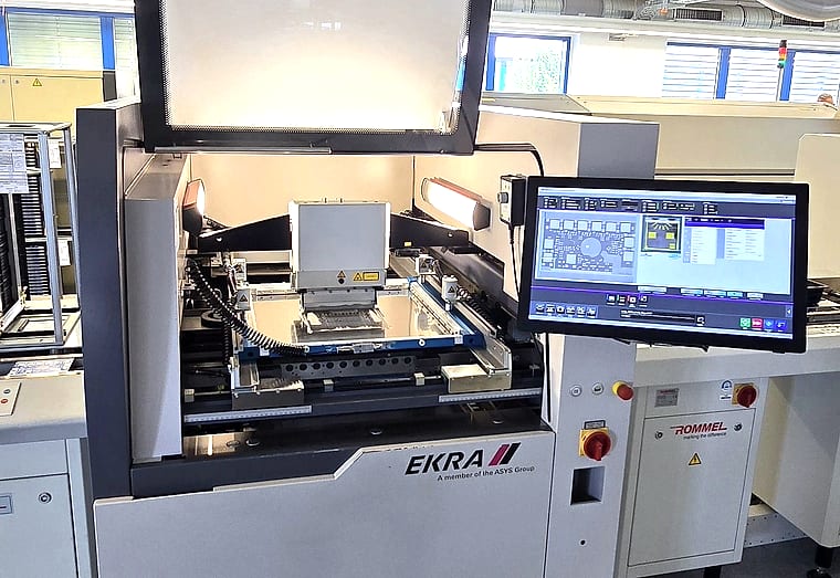
Applied in stencil printing with 2.5-D paste inspection as the most quality-critical step in SMD manufacturing.
Locations
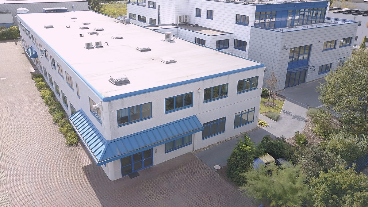
Berlin
DEProduction and administration
- Lot size
- Prototype to large-scale series
- Materials
- Ceramic substrates, printed circuit boards, thick-film pastes
- EKRA stencil printer with 2.5-D paste inspection
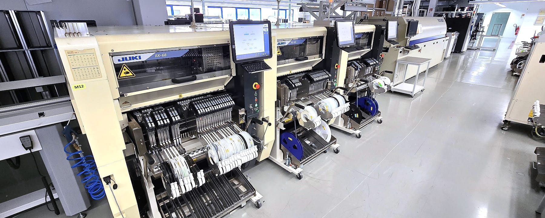
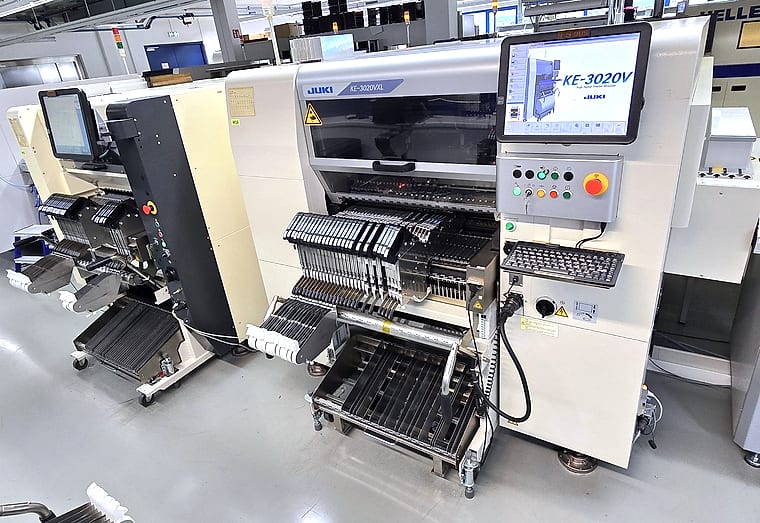
- JUKI FX-3, RX-6, RE-2060, KE-3020V SMD placement machines
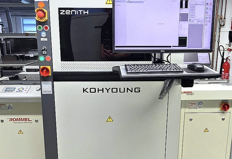
- Koh Young & Viscom 3D-AOI
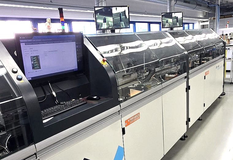
- Ersa selective soldering system (nitrogen)
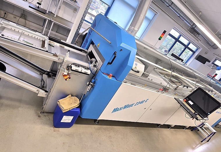
- SEHO encapsulated nitrogen wave soldering system
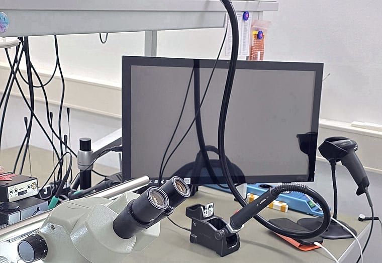
- JBC hand soldering and rework stations
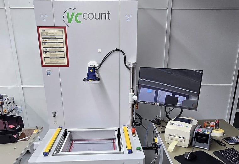
- X-ray counting system in incoming goods
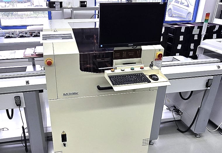
- Nutek laser marking system
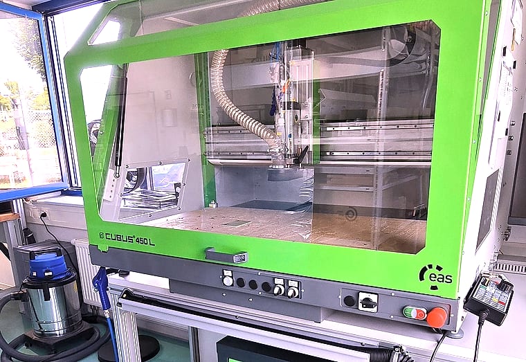
- 2 CNC milling machines
- 2 3D printers
- Reflow ovens (air/nitrogen)
- Screen printing system and firing oven (thick film)
- Laser trimming system
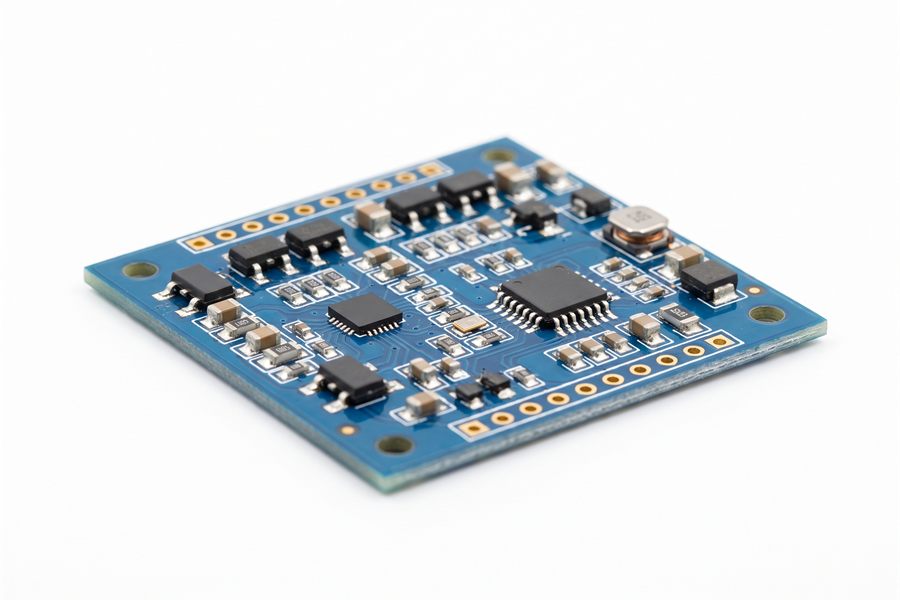
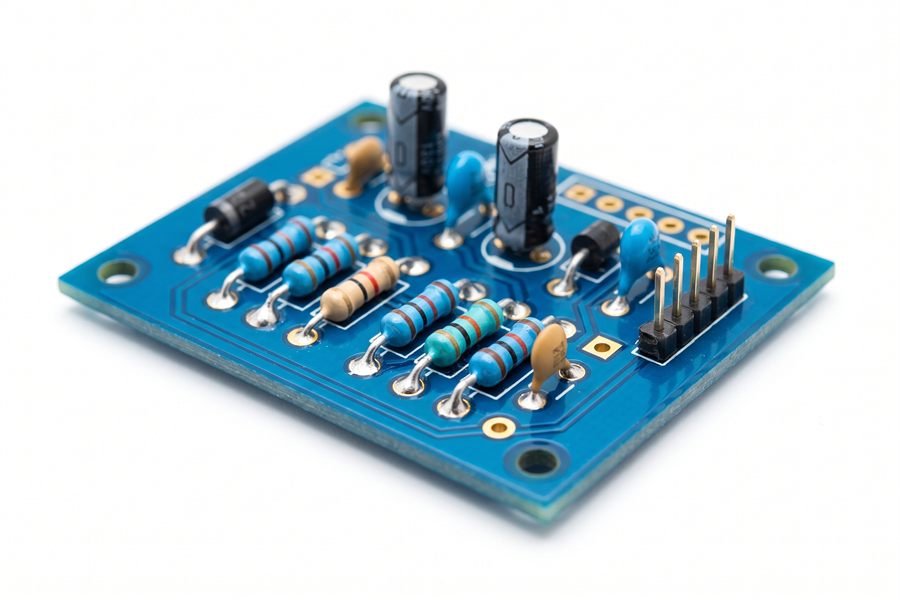
Assemblies
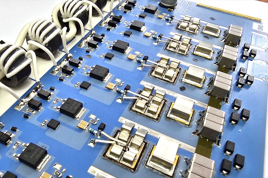
Inside the production


Industries
Processes & technical limits
| Processes | Tolerance | Max. part | Weight | Lot size | Materials |
|---|---|---|---|---|---|
| EMS (Electronics Manufacturing Services) - electronic assembly manufacturing and assemblyAssembly | – | – | – | Small series – Large series | Printed circuit boards, electronic components |
| SMD placement (Surface Mount Device)Assembly | – | – | – | – | electronic components, printed circuit boards |
| Reflow soldering in air or under nitrogenJoining | – | – | – | – | Solder paste, SMD components |
| THD placement (Through-Hole Device) with light-controlled placement tablesAssembly | – | – | – | – | wired components, printed circuit boards |
| Selective solderingJoining | – | – | – | – | wired components |
| Wave soldering (nitrogen wave soldering)Joining | – | – | – | – | wired components |
| Dip solderingJoining | – | – | – | – | wired components |
| Hand soldering & rework at microscope workstationsJoining | – | – | – | Prototypes/very small series | electronic components |
| Thick-film hybrid technology - conductor tracks and resistors applied by screen printing ontoSurface | Laser trimming to better than 0.1% | – | – | – | Ceramic substrate, Thick-film pastes |
| Laser trimming of thick-film resistorsSurface | better than 0.1% | – | – | – | Thick-film resistors on ceramic |
| High-voltage applications up to 30 kV (hybrid technology)Assembly | – | – | – | – | Ceramic substrate |
| Stencil printing (solder paste application) with 2.5-D paste inspectionJoining | – | – | – | – | Solder paste |
| Automated optical inspection (AOI), measured in 3DTesting | – | – | – | – | – |
| Electrical functional testing to customer specifications including test adapters and softwareTesting | – | – | – | – | – |
| X-ray counting of components (incoming goods)Testing | – | – | – | – | – |
| Laser marking of assemblies (plain text, barcode, data matrix)Surface | – | – | – | – | Substrate, heat-resistant labels |
| CNC milling of workpiece carriers, soldering frames and test fixturesMachining | – | – | – | – | – |
| 3D printing of workpiece carriers, soldering frames and test fixturesAdditive | – | – | – | – | – |
| Design for Manufacturing & Testability (DFM/DFT) - test concept development by test engineerEngineering | – | – | – | – | – |
| Subcontracting - manufacturing with customer-supplied components and circuit boardsAssembly | – | – | – | – | Customer-supplied circuit boards, Customer-supplied components |
18 Anlagen & Maschinen
| Machine | Manufacturer / model | Quantity | Working area | Year built | Site |
|---|---|---|---|---|---|
| Stencil printer with integrated 2.5-D paste inspection | EKRA | – | – | – | Berlin |
| High-speed SMD placement machine | JUKI FX-3 | – | – | – | Berlin |
| High-speed SMD placement machine | JUKI RX-6 | – | – | – | Berlin |
| Flexible SMD placement machine | JUKI RE-2060 | – | – | – | Berlin |
| Flexible SMD placement machine | JUKI KE-3020V | – | – | – | Berlin |
| 3D automated optical inspection (AOI) | Koh Young | – | – | – | Berlin |
| 3D automated optical inspection (AOI) | Viscom | – | – | – | Berlin |
| Selective soldering system (under nitrogen) | Ersa | – | – | – | Berlin |
| Encapsulated nitrogen wave soldering system (dip soldering) | SEHO | – | – | – | Berlin |
| Soldering stations for hand soldering & rework | JBC | – | – | – | Berlin |
| X-ray counting system (incoming goods) | – | – | – | – | Berlin |
| Laser marking system | Nutek | – | – | – | Berlin |
| CNC milling machine | – | 2 | – | – | Berlin |
| 3D printer | – | 2 | – | – | Berlin |
| Screen printing system for thick-film hybrid technology | – | – | – | – | Berlin |
| Firing oven for thick film (approx. 800 °C) | – | – | – | – | Berlin |
| Laser trimming system (laser trimming) | – | – | – | – | Berlin |
| Reflow ovens (air/nitrogen) | – | – | – | – | Berlin |
Additional services
Quality
Manufacturing is certified to DIN EN ISO 9001:2015 (TÜV Rheinland); ESD-protected production areas, climate-controlled printing processes as well as 3D-AOI and electrical functional testing including test adapters and software apply. Two lines operate with a Cogiscan traceability system for seamless traceability.
| Evidence | Berlin |
|---|---|
| ISO 9001 |
History
- 1991
Foundation; specialization in thick-film hybrid technology
- 2000
Initial certification to ISO 9001
- 2024
Re-certification to ISO 9001:2015 by TÜV Rheinland (valid until 18.12.2027)