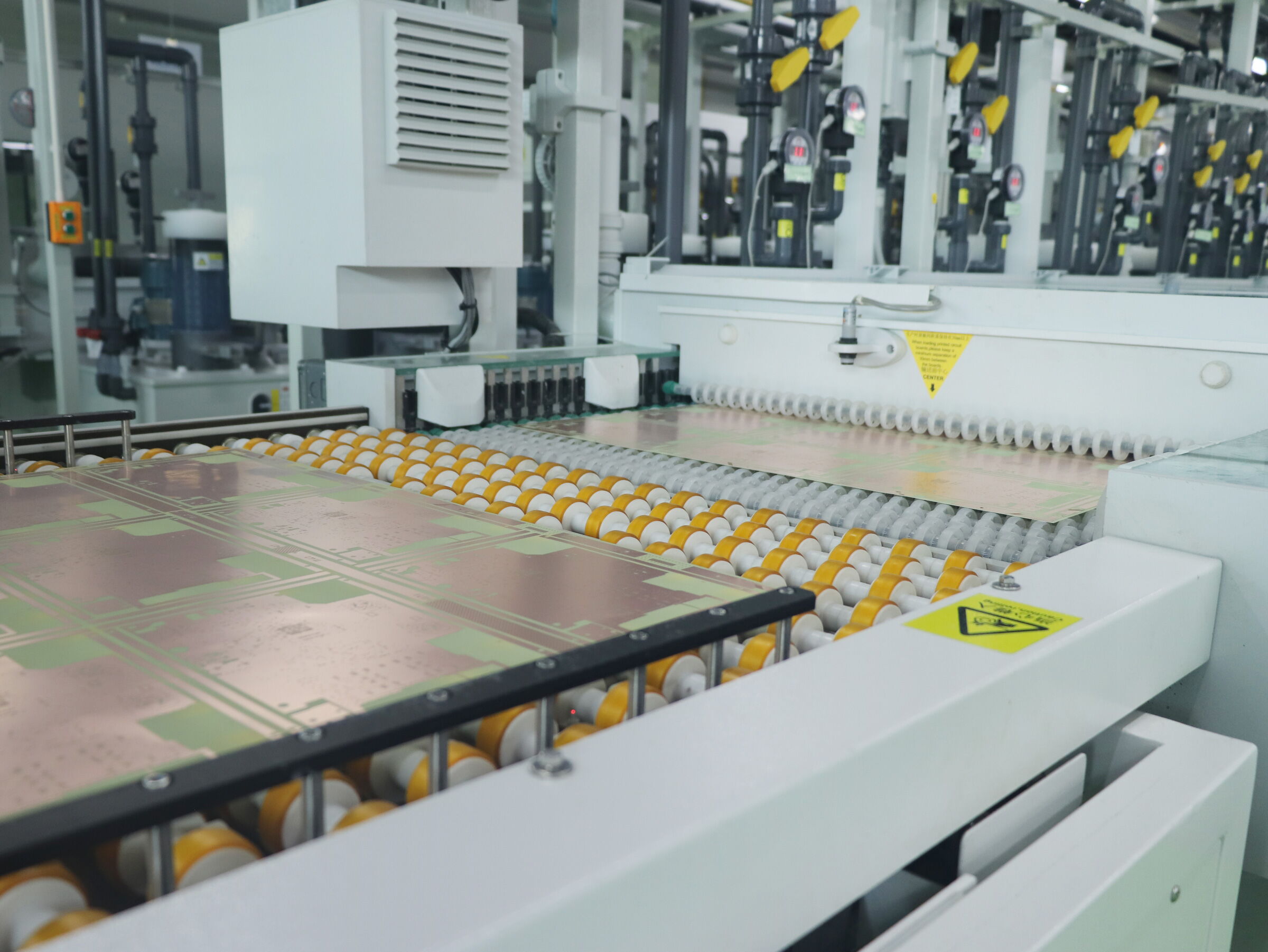
PCB manufacturer: Multilayer, HDI, RF, Rigid-Flex, IMS and Heavy Copper PCBs from prototype to series production

Sunshine PCB GmbH
Remscheid · Chemnitz · Shenzhen · Jiujiang · PenangNew on Amplifa
About Sunshine PCB
Sunshine PCB GmbH is a German PCB manufacturer with headquarters and production in Remscheid and, since 2013, part of the publicly listed Sunshine Global Circuits Ltd. in China. The portfolio covers single-sided and double-sided PCBs, multilayer boards up to 48 layers, as well as HDI, high-frequency (up to 77 GHz), rigid-flex, IMS and heavy-copper PCBs with up to 210 µm copper. Production uses FR4 in various specializations (including halogen-free, high Tg, low Dk/Df), polyimide, aluminium cores, ceramics and VLP copper foils. Manufacturing technologies include direct imaging, laser drilling of microvias, camera-controlled CNC milling, impedance-controlled fabrication and testing via AOI, electrical bare-board tests and impedance measurement. Customer industries include the automotive industry, medical technology, telecommunications, aerospace, power electronics, industrial engineering, LED/lighting and communication electronics. Prototypes and small series are manufactured at the Remscheid site; series production takes place at the Chinese plants in Shenzhen and Jiujiang as well as in Penang, Malaysia, with a total production capacity of over 80,000 m² per month.
- Site
- Remscheid
- Processes
- Single-sided PCBs, Double-sided PCBs, Multilayer PCBs up to 48 layers, Standard PCBs (rigid PCBs), Heavy copper PCBs, HDI PCBs (microvias, blind/buried vias), Rigid-flex PCBs, IMS PCBs (Insulated Metal Substrate)
- Materials
- FR4.0 standard material (brominated), FR4.1 standard material (halogen-free), FR4 with high Tg value, FR4 with low Dk/Df value, Copper, Polyimide (flex), Aluminium (IMS heat sink), Ceramic (PCBs)
- Certificates
- DIN EN ISO 9001:2015, DIN EN ISO 14001:2015, DIN EN ISO 50001:2018, UL, ISO 9001:2015 / ISO 14001 / IATF 16949:2016 / ISO 13485:2016 / ISO 45001:2018 /, AS9100 (Jiujiang), ISO 9001:2015 (Penang, Malaysia), ISO 9001, ISO 14001, ISO 50001, IATF 16949, ISO 13485, ISO 45001, EN 9100 (AS9100)
- Founded
- 1969 (Stan
- Employees
- approx. 40 (Remschei
- Industries
- Automotive industry, Medical technology, Telecommunications, Aerospace, Power electronics/Energy technology, Industrial engineering
- 01
Data preparation & DFM support
- 02
Engineering (stack-ups, impedance modelling, material selection)
- 03
Exposure / direct imaging
- 04
Etching & continuous plating
- 05
Lamination & drilling (incl. laser microvias)
- 06
Machining (CNC milling, scoring, depth milling)
- 07
Testing (AOI, electrical tests, impedance measurement, laboratory analysis)
- 08
Shipping with test documentation
Materials & Technologies
FR4 Standard (brominated)
Glass-fibre-reinforced epoxy resin as the standard base material for rigid PCBs.
FR4 halogen-free
Halogen-free standard base material for applications with increased environmental requirements.
FR4 with high Tg value
For higher thermal loads during operation and the lamination process.
FR4 with low Dk/Df
Low-loss base material for high-speed and high-frequency applications.
Copper / Heavy Copper
Traces and heavy-copper layers up to 210 µm for high currents and power electronics.
Polyimide
Flexible base material for rigid-flex and flexible PCBs.
Aluminium (IMS)
Aluminium heat sink with dielectric layer for improved heat dissipation in high-power LEDs and power electronics.
Ceramic
Base material for ceramic PCBs at the Penang site.
VLP copper foils (low profile)
Low-profile copper foils combined with ultra-low-loss materials for RF PCBs.
Production Sites
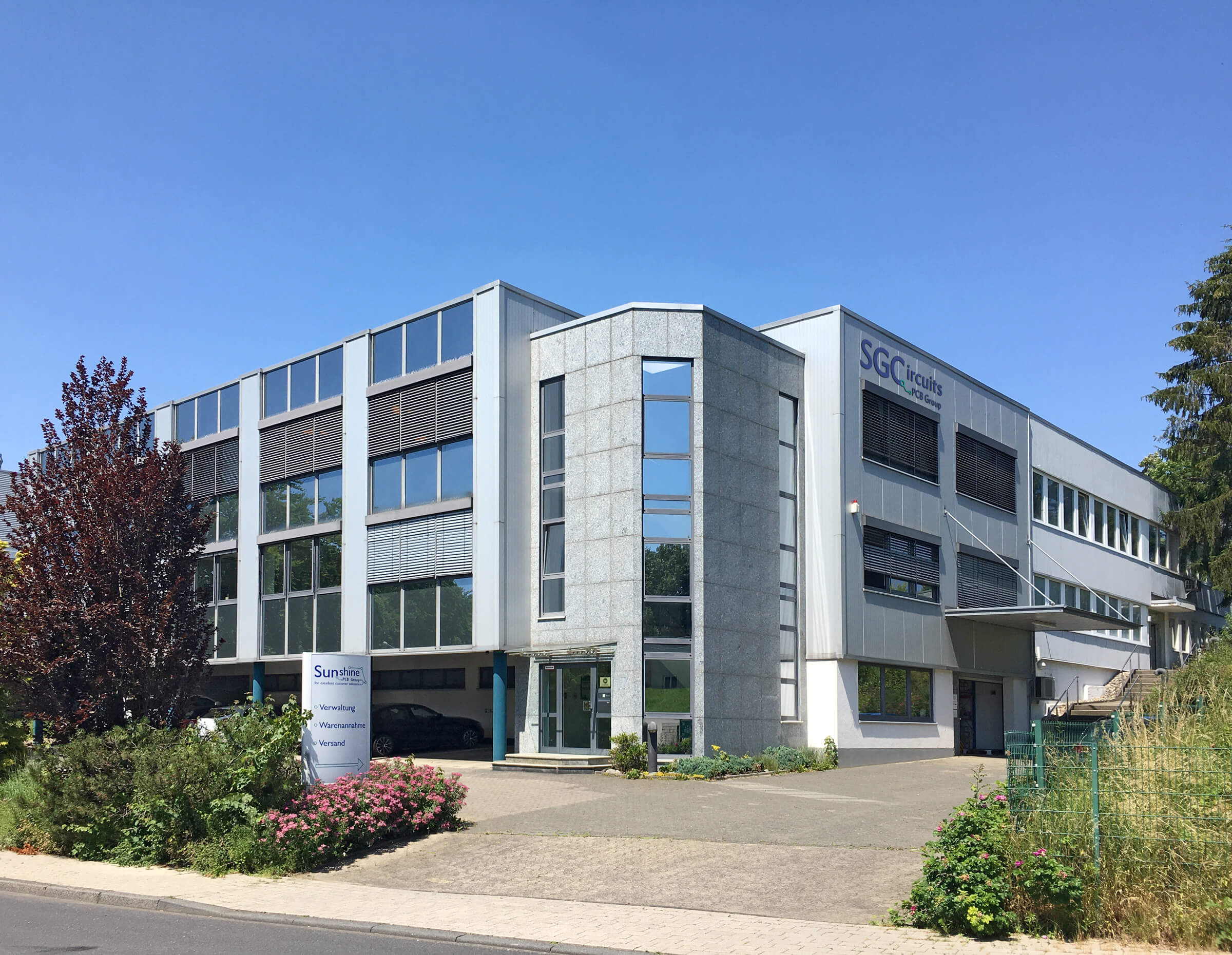
Remscheid
DEHeadquarters and production (prototypes, small series)
- Part weight / size
- Multilayer 2–12 layers, HDI, rigid-flex, IMS
- Lot size
- Prototype to small series
- Materials
- FR4, copper, polyimide, aluminium
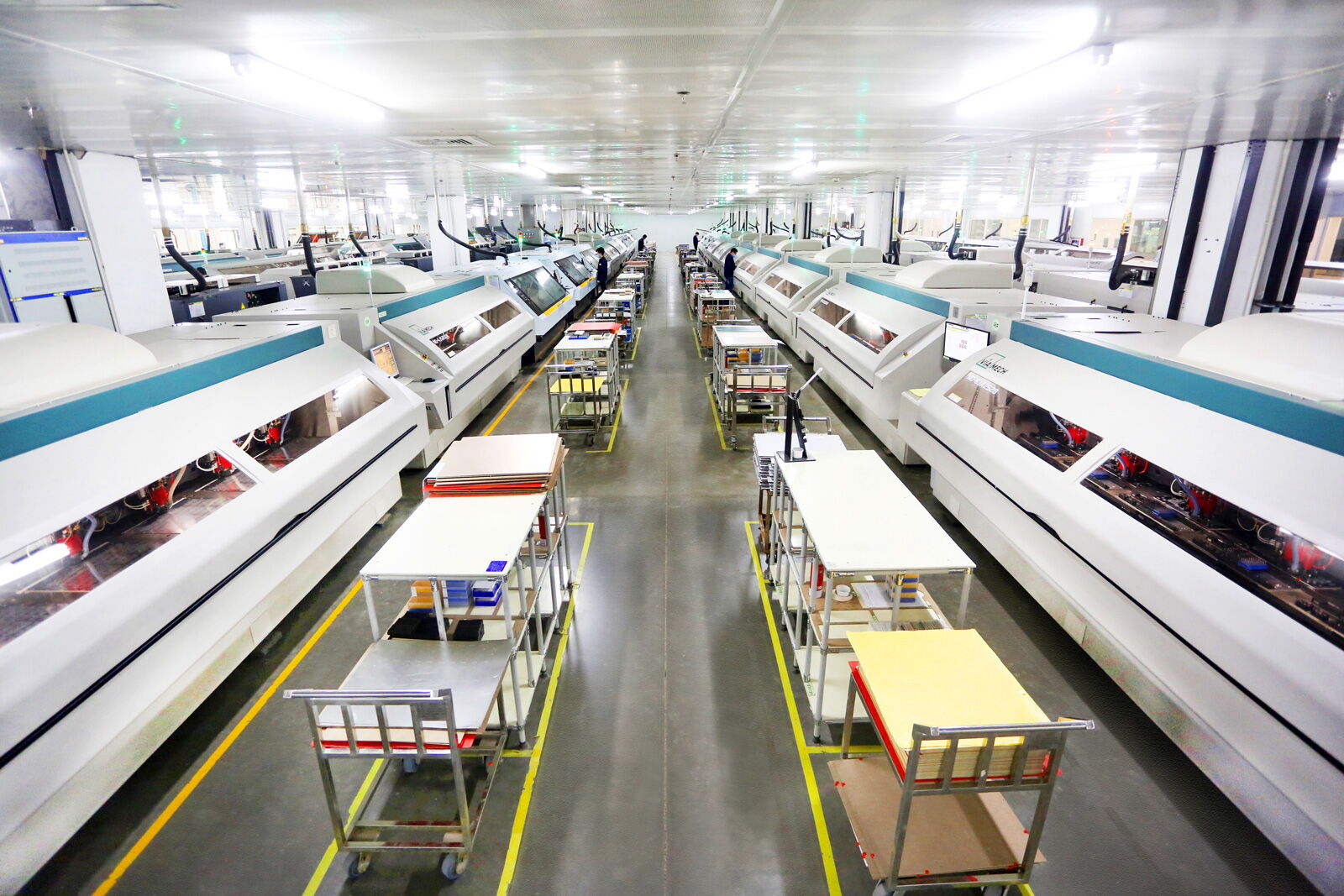
- Camera-controlled CNC milling machines
- Direct imaging systems
- Inline AOI systems
Chemnitz
DESales location
Shenzhen
CNProduction
- Part weight / size
- Multilayer 2–48 layers, HDI, high speed
- Lot size
- Prototype to large series, QTA 10 working days
- Materials
- FR4, copper
- Direct imaging systems
- Vertical continuous plating systems
- Vacuum-assisted epoxy resin filling systems
- Automated handling systems
Jiujiang 1
CNProduction
- Part weight / size
- Multilayer 2–16 layers, heavy copper, RF, rigid-flex
- Lot size
- Prototype to large series, QTA 10 working days
- Materials
- FR4, copper, polyimide
- Spray coating systems
- Inline AOI systems
Jiujiang 2
CNProduction (highly automated plant)
- Part weight / size
- Multilayer 2–26 layers, heavy copper 3–6 oz, backpanels, HDI
- Lot size
- Large series
- Materials
- FR4, copper
- Automated PCB production line with intelligent manufacturing
- SLP/mSAP line
Penang
MYProduction (Vision Industries Sdn. Bhd.)
- Part weight / size
- Multilayer 2–12 layers, RF/microwave, ceramic PCBs
- Lot size
- Prototype to series
- Materials
- Ceramic, FR4, copper
PCB Technologies
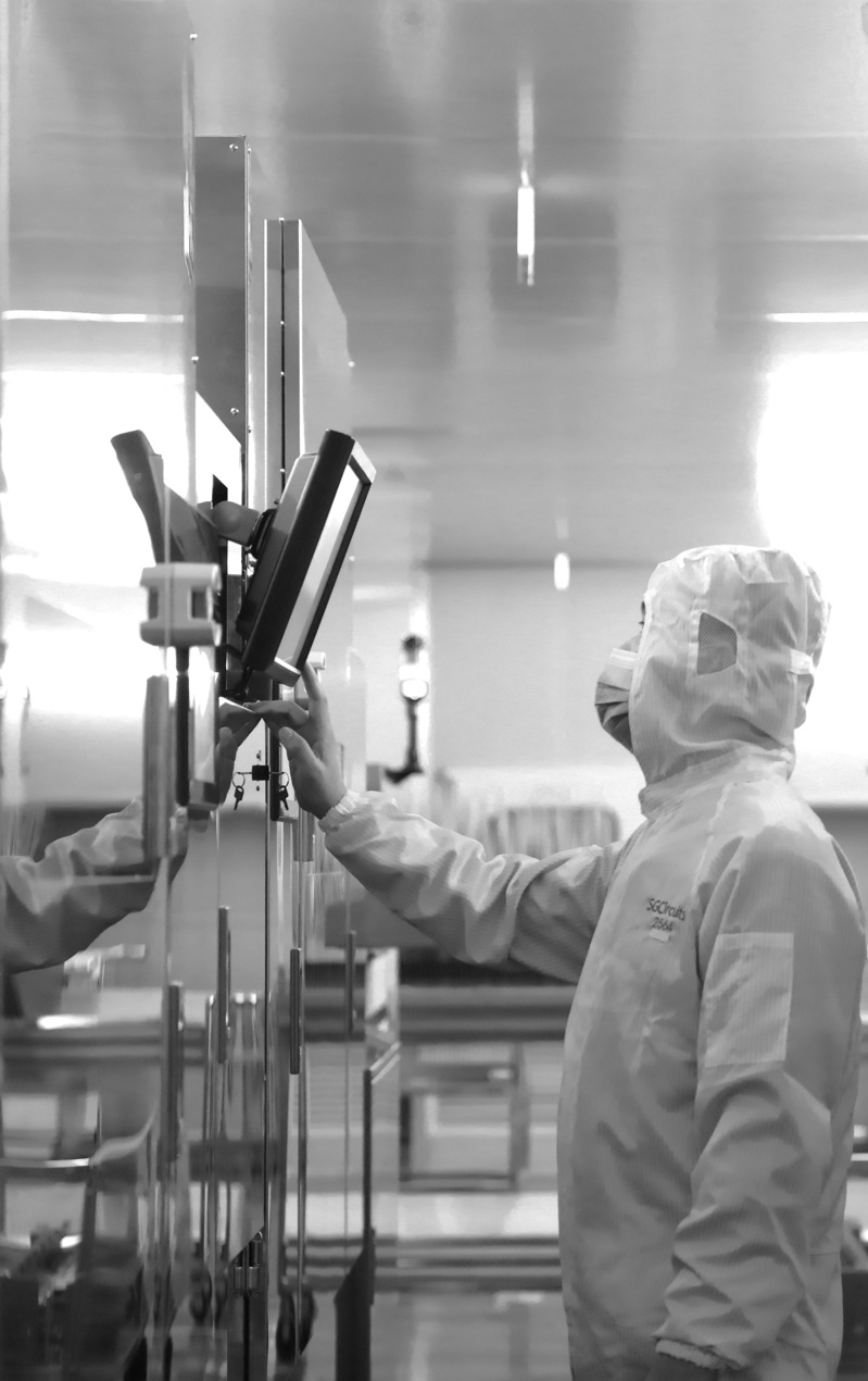
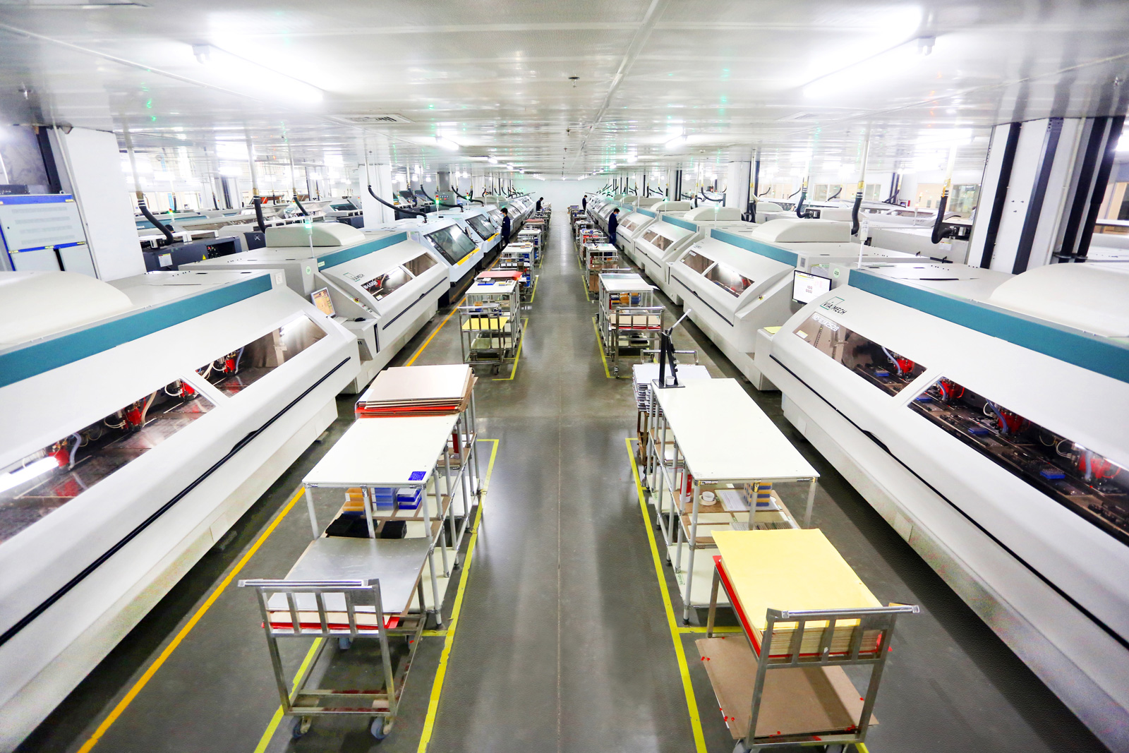
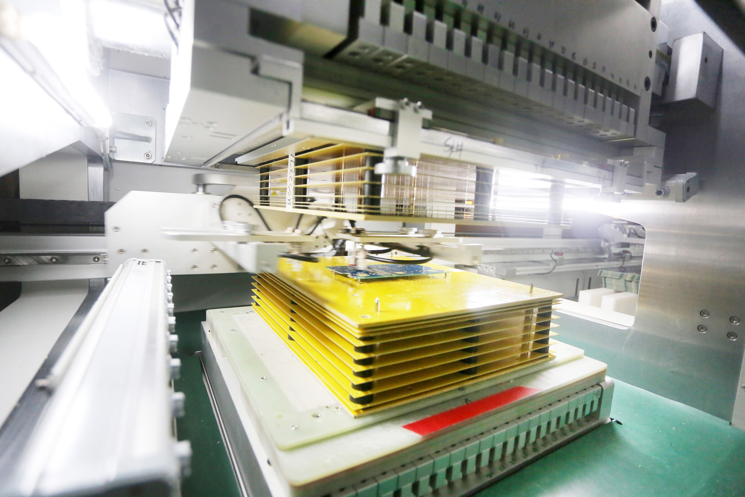
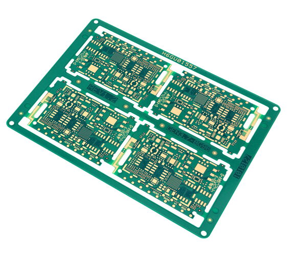
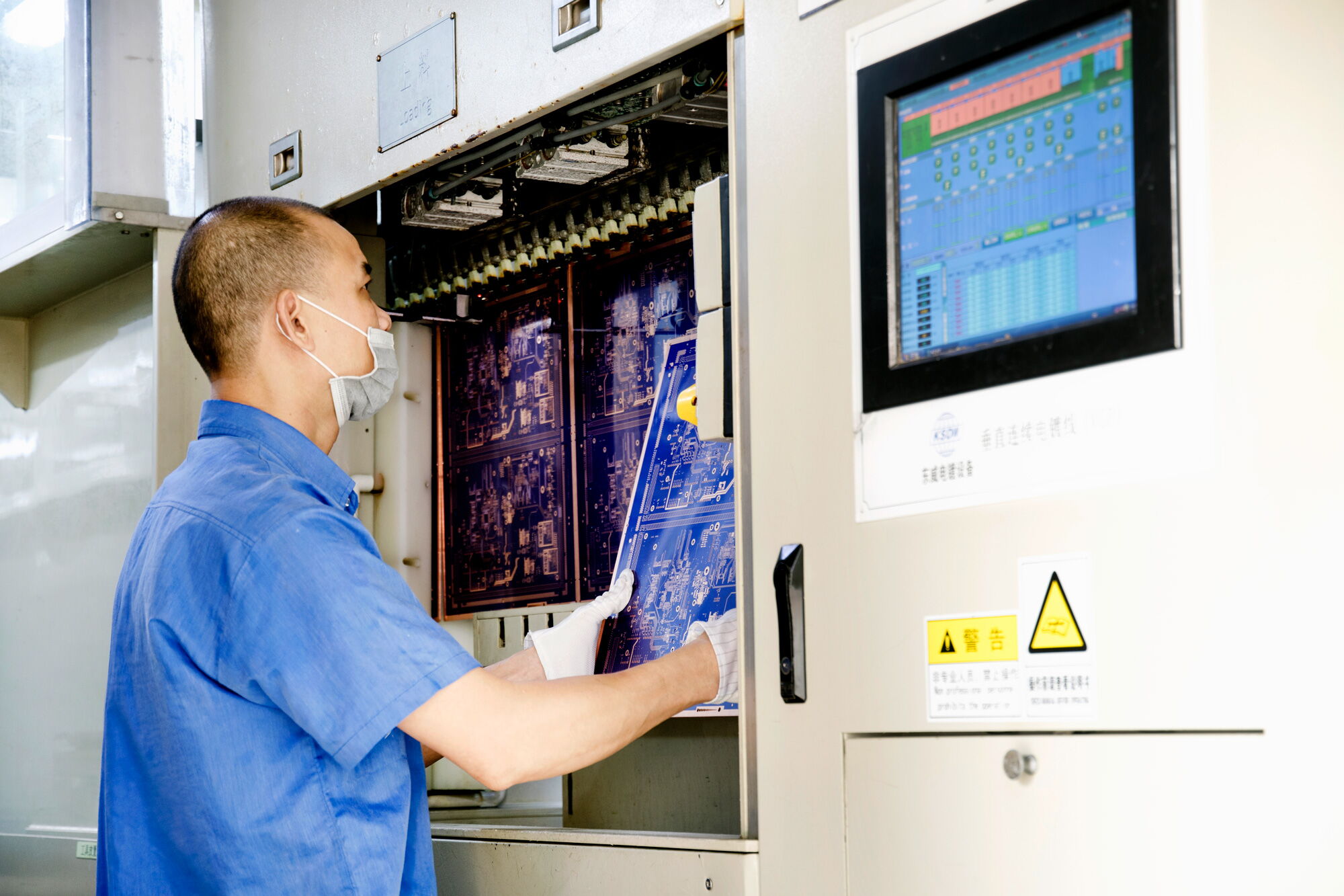
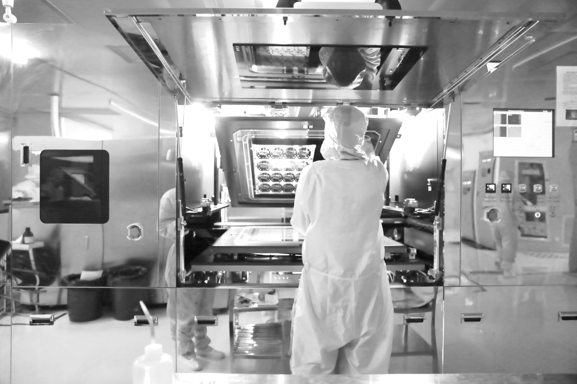
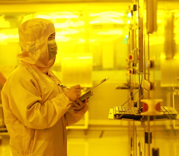
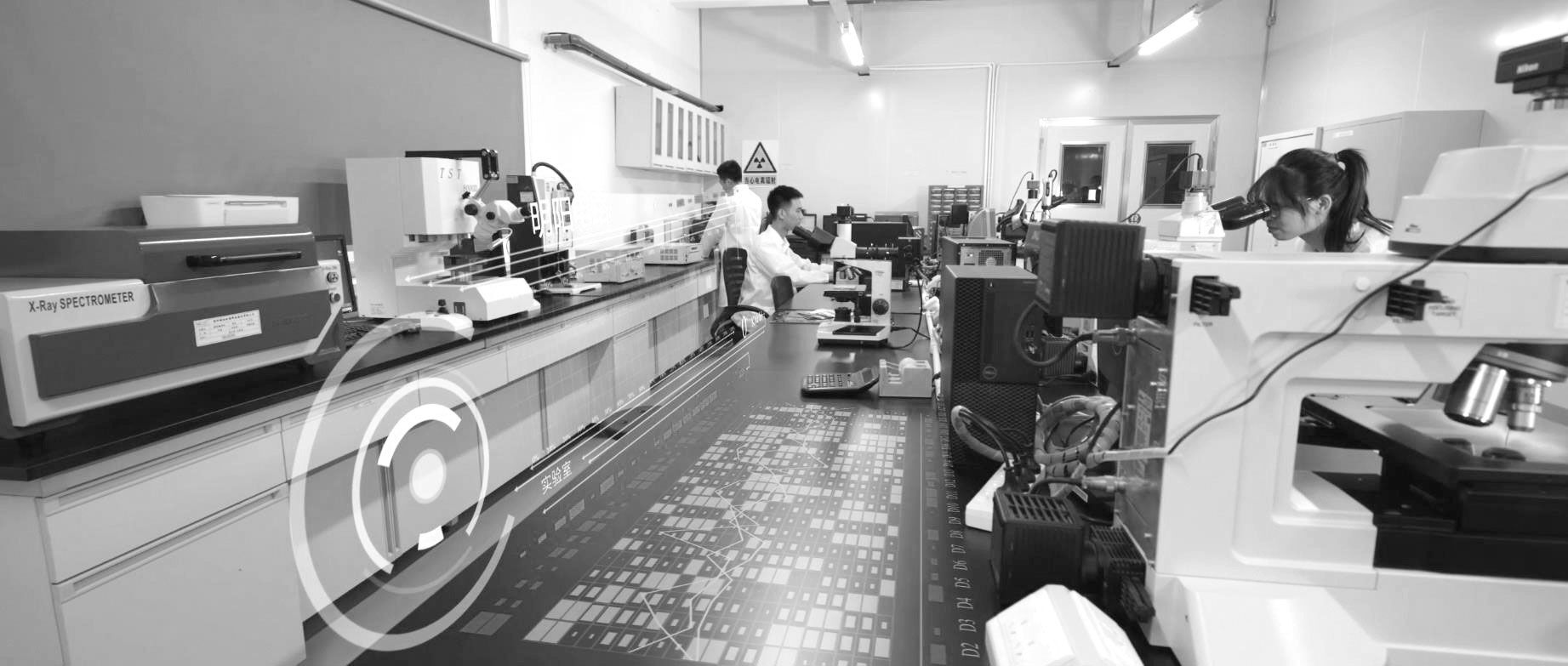
Inside the production
Industries
Processes & technical limits
| Processes | Tolerance | Max. part | Weight | Lot size | Materials |
|---|---|---|---|---|---|
| Single-sided PCBsPCB manufacturing | – | – | – | – | Copper, FR4 |
| Double-sided PCBsPCB manufacturing | – | – | – | – | Copper, FR4 |
| Multilayer PCBs up to 48 layersPCB manufacturing | Impedance tolerance +/-5% | – | – | – | FR4.0, FR4.1 halogen-free, FR4 with high Tg, FR4 with low Dk/Df, Copper |
| Standard PCBs (rigid PCBs)PCB manufacturing | – | – | – | – | FR4 |
| Heavy copper PCBsPCB manufacturing | – | – | – | – | Copper, FR4 (prepregs) |
| HDI PCBs (microvias, blind/buried vias)PCB manufacturing | – | – | – | – | Copper, FR4 |
| Rigid-flex PCBsPCB manufacturing | – | 3.0 mm final thickness | – | – | Polyimide, Copper, FR4 |
| IMS PCBs (Insulated Metal Substrate)PCB manufacturing | – | – | – | – | Aluminium, Copper, Prepreg |
| High-frequency PCBs (RF, up to 77 GHz)PCB manufacturing | – | – | – | – | VLP copper foils, High-frequency base materials |
| Prototype manufacturing / small seriesPCB manufacturing | – | 610 mm × 450 mm | – | – | FR4 |
| Ceramic PCBsPCB manufacturing | – | – | – | – | Ceramic |
| Flexible PCBsPCB manufacturing | – | – | – | – | Polyimide |
| BackpanelsPCB manufacturing | – | – | – | – | FR4 |
| SLP/mSAP line (substrate-like PCB, modified semi-additive process)PCB manufacturing | – | – | – | – | – |
| Machining: scoring/jump scoring, controlled depth milling, back drillingPCB manufacturing | – | – | – | – | FR4, Copper |
| Laser drilling of microviasPCB manufacturing | Diameter 0.05–0.15 mm | – | – | – | Copper, FR4, Polyimide |
| Impedance measurement with TDR or network analyserTesting | – | – | – | – | – |
| AOI (inner/outer layers), electrical bare-board tests, final visual inspection, laboratory testsTesting | – | – | – | – | – |
| DFM support, stack-up design, impedance modelling, material selectionEngineering | – | – | – | – | – |
| 3D printing / additive processes (R&D, Green Manufacturing Technology Center)Additive | – | – | – | – | – |
8 Anlagen & Maschinen
| Machine | Manufacturer / model | Quantity | Working area | Year built | Site |
|---|---|---|---|---|---|
| Camera-controlled CNC milling machines | – | – | – | – | Remscheid |
| Direct imaging systems | – | – | – | – | – |
| Vertical continuous plating systems | – | – | – | – | – |
| Inline AOI systems | – | – | – | – | – |
| Vacuum-assisted epoxy resin filling systems | – | – | – | – | – |
| Spray coating systems | – | – | – | – | – |
| Automated handling systems | – | – | – | – | – |
| Automated PCB production line | – | – | – | 2022 | Jiujiang 2 |
Additional services
Quality & Certifications
Quality assurance includes 100 % AOI on inner and outer layers, 100 % electrical bare-board netlist testing, final visual inspection as well as impedance measurements using TDR or a network analyser. At the Chinese sites, a failure analysis laboratory with SEM/EDX, thermal shock, CAF and ion chromatography is available; test reports, first-article inspections and customer audits are possible.
| Evidence | Remscheid | Shenzhen | Jiujiang | Penang |
|---|---|---|---|---|
| ISO 9001 | ||||
| ISO 14001 | ||||
| ISO 50001 | ||||
| IATF 16949 | ||||
| ISO 13485 | ||||
| ISO 45001 | ||||
| EN 9100 (AS9100) | ||||
| UL |
Company History
- 1969
Start of PCB manufacturing at the Remscheid site
- 2001
Founding of Sunshine Global Circuits Co., Ltd. and start of production in Shenzhen, China
- 2007
Certification of the environmental management system (ISO 14001) in Shenzhen
- 2011
Opening of a sales location in the USA
- 2012
Opening of a sales location in Chemnitz, Germany
- 2013
Acquisition of the Remscheid production site and renaming to Sunshine PCB GmbH; start of production in Jiujiang
- 2018
IPO, listed on the Shenzhen Stock Exchange (300739); founding of the Green Manufacturing Technology Center (GMTC) in Shenzhen
- 2019
Total production capacity exceeds 80,000 m² per month, over 2,100 employees worldwide
- 2020
Jiujiang plant certified to ISO 45001 and recognised as a 'Green Factory'; installation of a geothermal system in Jiujiang
- 2021
Start of production at the second manufacturing plant in Jiujiang
- 2022
Automated PCB line with intelligent manufacturing in Jiujiang II; construction start of a new factory in Zhuhai
- 2023
Acquisition of the PCB manufacturer Vision Industries Sdn. Bhd. in Penang, Malaysia