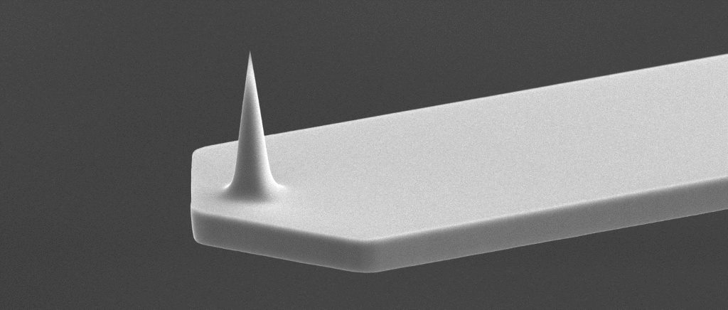
Manufacturing of SPM probe tips, probe tip characterizers and silicon-based 3D MEMS components.

Team Nanotec GmbH
Villingen-SchwenningenNew on Amplifa
About Team Nanotec
Team Nanotec GmbH was founded in 1997 as a spin-off of IBM Germany and develops and manufactures silicon-based micro and nano components at its headquarters in Villingen-Schwenningen. The portfolio includes SPM probe tips (AFM cantilevers) for scanning probe microscopy, probe tip characterizers for quantitative 3D AFM, MEMS-based beam-shaping apertures as well as stencil masks. In addition to standard products, the company develops and manufactures custom cantilevers and probe tips. Products are manufactured, among other processes, in batch processes from single-crystal silicon, silicon nitride and metals; the MEMS apertures are characterized by controlled profiles, smooth sidewalls and small corner radii. Customers come from scanning probe microscopy, metrology, material characterization and micro/nano fabrication. To ensure warranty coverage, SPM products are measured in-house with an electron beam microscope.
- Site
- Villingen-Schwenningen
- Processes
- Micro and nano fabrication (SPM tips, characterizers, 3D MEMS), Batch manufacturing of silicon SPM tips (AFM cantilevers/probe tips), Production of custom cantilevers and probe tips, Stencil mask technology, MEMS manufacturing of beam-shaping apertures with controlled profiles,, Production of probe tip characterizers (e.g. I²FSR, CDR probes), Measurement of SPM products with electron beam microscope (warranty-relevant, Custom cantilever and probe tip development and manufacturing
- Materials
- Silicon (single crystal, high quality single crystal silicon), Silicon nitride, Metals
- Founded
- 1997
- Industries
- Scanning probe microscopy (SPM/AFM), Metrology, Material characterization, Micro and nano fabrication
- 01
Development of custom cantilevers and MEMS components
- 02
Micro and nano fabrication (batch manufacturing)
- 03
Electron beam microscopic measurement and inspection
- 04
Shipping ex works
Sites
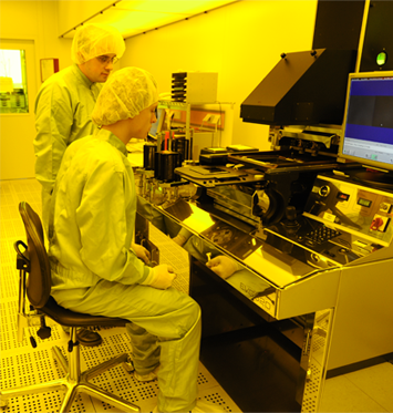
Villingen-Schwenningen
DEHeadquarters, development and manufacturing
- Materials
- Silicon, silicon nitride, metals
- Electron beam microscope (measurement)
Industries
Processes & technical limits
| Processes | Tolerance | Max. part | Weight | Lot size | Materials |
|---|---|---|---|---|---|
| Micro and nano fabrication (SPM tips, characterizers, 3D MEMS)Engineering | – | – | – | – | Silicon, Silicon nitride, Metals |
| Batch manufacturing of silicon SPM tips (AFM cantilevers/probe tips)Engineering | – | – | – | – | Silicon (single crystal) |
| Production of custom cantilevers and probe tipsEngineering | – | – | – | – | Silicon |
| Stencil mask technologyEngineering | – | – | – | – | Silicon |
| MEMS manufacturing of beam-shaping apertures with controlled profiles,Engineering | – | – | – | – | Silicon, Silicon nitride, Metals |
| Production of probe tip characterizers (e.g. I²FSR, CDR probes)Engineering | – | – | – | – | Silicon |
| Measurement of SPM products with electron beam microscope (warranty-relevantInspection | – | – | – | – | – |
Additional services
History
- 1997
Foundation of Team Nanotec GmbH as a spin-off of IBM Germany