
Manufacturer of photomasks, silicon stencil masks and molds for nanoimprint lithography for the semiconductor industry

Tekscend Photomask Corp.
Tokyo · DresdenNew on Amplifa
About Tekscend Photomask
Tekscend Photomask Corp. is a supplier of photomasks for semiconductor manufacturing headquartered in the Shiodome City Center in Tokyo. The product portfolio comprises photomasks for semiconductors, photomasks for various other applications, silicon stencil masks as well as molds for nanoimprint lithography (NIL). Manufacturing is based on state-of-the-art microstructuring technology; at the European site in Dresden, the first multibeam mask writer in Europe was presented together with IMS Nanofabrication, enabling photomask writing with multibeam technology. In 2025, Tekscend Photomask Japan commissioned a new NIL production line and announced investments in photomask writing capacity in Europe as well as a new plant in Singapore. The company supplies the semiconductor industry worldwide and, according to its own statement, sees itself as the first choice for its customers.
- Site
- 105-7133 Tokyo
- Processes
- Photomask Manufacturing (Photomasks for Semiconductors), Molds for Nanoimprinting / Nanoimprint Lithography (NIL), Silicon Stencil Mask, Photomasks for Various Applications, Multibeam Mask Writing (Mask Writer, Cooperation with IMS Nanofabrication), Photomasks for semiconductors, Molds for nanoimprinting (NIL), Silicon stencil masks
- Materials
- Silicon, Multibeam Mask Writing, Nanoimprint Lithography
- Industries
- Semiconductor Industry
- 01
Photomask writing (multibeam mask writer)
- 02
Microstructuring
- 03
Quality inspection
- 04
Delivery to semiconductor manufacturers
Materials & Processes
Silicon
Base material for silicon stencil masks and photomasks.
Multibeam Mask Writing
Writing process for photomasks in cooperation with IMS Nanofabrication, presented as the first multibeam mask writer in Europe in Dresden.
Nanoimprint Lithography
Process for the manufacture of molds for nanoimprinting, with a new production line in Japan since 2025.
Locations
Tokyo
JPHeadquarters
Dresden
DEEuropean site with photomask writing capacity
- Materials
- Silicon
- Multibeam Mask Writer (IMS Nanofabrication)
Singapore
SGNew plant (ground-breaking 2025)
Products
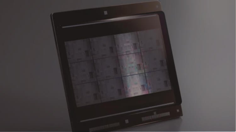
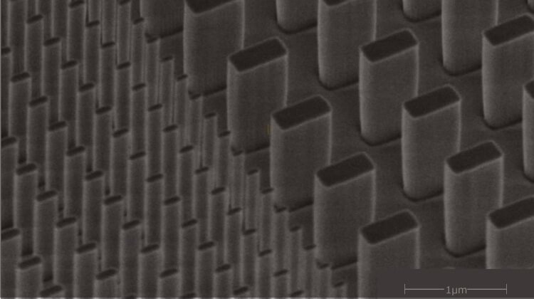
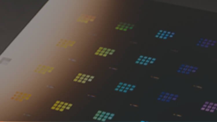
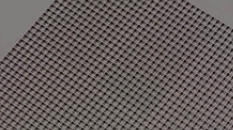
Inside the production


Industries
Processes & technical limits
| Processes | Tolerance | Max. part | Weight | Lot size | Materials |
|---|---|---|---|---|---|
| Photomask Manufacturing (Photomasks for Semiconductors)Engineering | – | – | – | – | Silicon |
| Molds for Nanoimprinting / Nanoimprint Lithography (NIL)Engineering | – | – | – | – | – |
| Silicon Stencil MaskEngineering | – | – | – | – | Silicon |
| Photomasks for Various ApplicationsEngineering | – | – | – | – | – |
| Multibeam Mask Writing (Mask Writer, Cooperation with IMS Nanofabrication)Engineering | – | – | – | – | – |
1 Anlagen & Maschinen
| Machine | Manufacturer / model | Quantity | Working area | Year built | Site |
|---|---|---|---|---|---|
| Multibeam Mask Writer | IMS Nanofabrication | – | – | – | Dresden (Europe) |
Additional services
History
- 2024
Joint presentation of the first multibeam mask writer in Europe with IMS Nanofabrication at AMTC Dresden (11.11.2024).
- 2024
Partnership agreement with Shiga Lakes (26.12.2024).
- 2025
Introduction of new corporate MVV (01.04.2025).
- 2025
Commissioning of a new nanoimprint lithography (NIL) production line in Japan (15.07.2025).
- 2025
Capacity expansion in Europe through strategic investment in photomask writing (21.07.2025).
- 2025
Ground-breaking ceremony for a new plant in Singapore (31.10.2025).
- 2026
MOU on investment promotion with Icheon City, South Korea (30.03.2026).
- 2026
Exhibition and presentation at NNT 2026 (07.10.2026).