
Development, manufacturing and distribution of Contact Image Sensors (CIS) for industrial inspection and scanning applications

Tichawa Vision GmbH
Friedberg (DE)New on Amplifa
About Tichawa Vision
Tichawa Vision GmbH develops, manufactures and distributes optical and electronic components and devices with a focus on Contact Image Sensors (CIS). These compact line cameras for direct mounting on the object to be inspected typically consist of a sensor line, a SELFOC lens and a light source, and are manufactured up to a scan width of 4 m. In addition to standard products such as MXCIS, VUCIS and BDCIS, the company offers modified and custom CIS solutions as well as software development. As with CCD and CMOS cameras, the sensor pixels are made of silicon with a sensitivity maximum in the near infrared. Resolutions range from 25 dpi (pixel pitch 1.016 mm) to 2400 dpi (pixel pitch 10.6 μm), and the standard working distance is 10 mm. Customers come from printing and scanning technology, the semiconductor industry (wafer inspection), digital printing and automation technology. The main site is located in Friedberg near Augsburg; the managing directors are Dr. Nikolaus Tichawa and Krisztina Tichawa.
- Site
- Friedberg
- Processes
- Development, manufacturing and distribution of optical and electronic components and devices, Custom CIS solutions / modified standard products (Contact Image Sensors), CIS with resolutions from 25 dpi (pixel pitch 1.016 mm) to 2400 dpi (pixel pitch 10.6 μm),, BDCIS - Basic Distance CIS (increased working distance, resolution up to 240 dpi as standard,, MXCIS - Maxi CIS (all-in-one: illumination, optics, sensors, data preprocessing; resolutions 100, VUCIS - VARI Universal CIS (16 illumination geometries, 10 illumination colors, 8 optics with, Modified and custom CIS solutions, Software development
- Materials
- Silicon (sensor pixels, typical for CCD/CMOS), Silicon, Contact Image Sensor Technology, Integrated Illumination Technology
- Certificates
- DIN EN ISO 9001:2015, ISO 9001
- Founded
- 1997
- Industries
- Printing and scanning technology, Semiconductor industry (wafer inspection), Automation technology, Digital Printing
- 01
Engineering and software development
- 02
Manufacturing of the CIS modules
- 03
Distribution and customer service
- 04
Support
Materials & Technology
Silicon
As with CCD and CMOS cameras, the sensor pixels of the CIS are made of silicon with a sensitivity maximum in the near infrared.
Contact Image Sensor Technology
Compact line camera with 1:1 imaging via a SELFOC lens, scan width up to 4 m and a constant viewing angle across the entire width.
Integrated Illumination Technology
The CIS supports multiplexed operation of up to six light sources, with colors from IR to UV.
Locations
Friedberg
DEMain site: development, manufacturing and distribution
- Materials
- Silicon (sensor pixels)
Products & Sensors
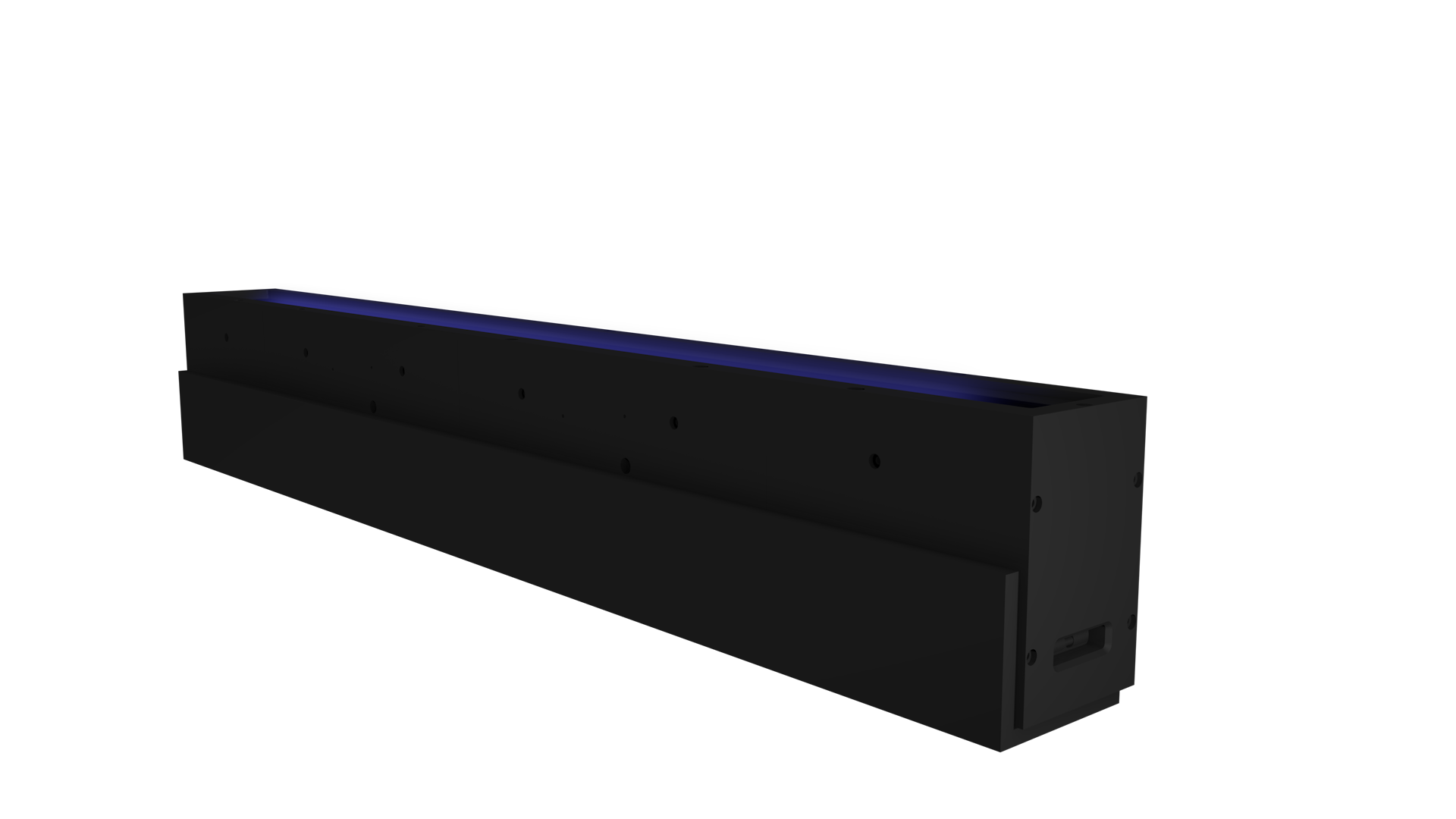
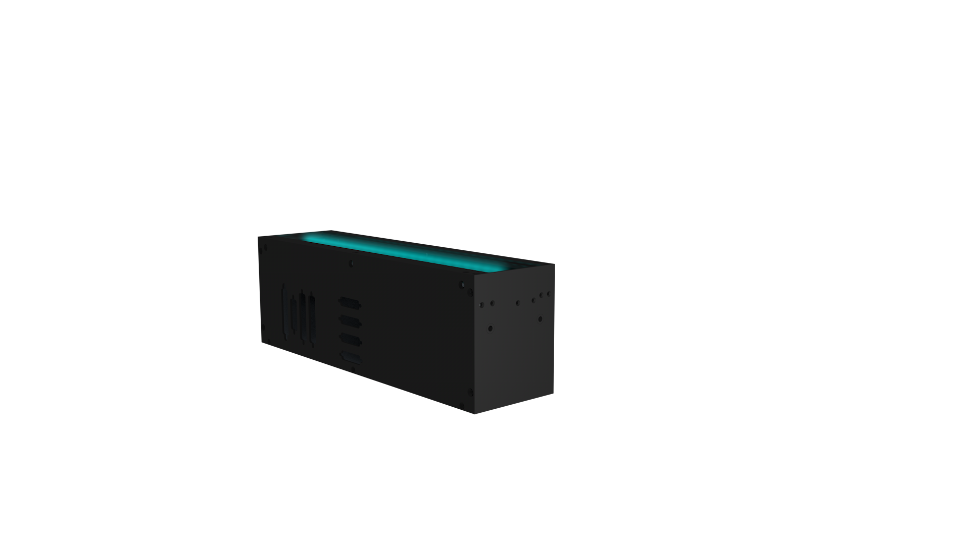
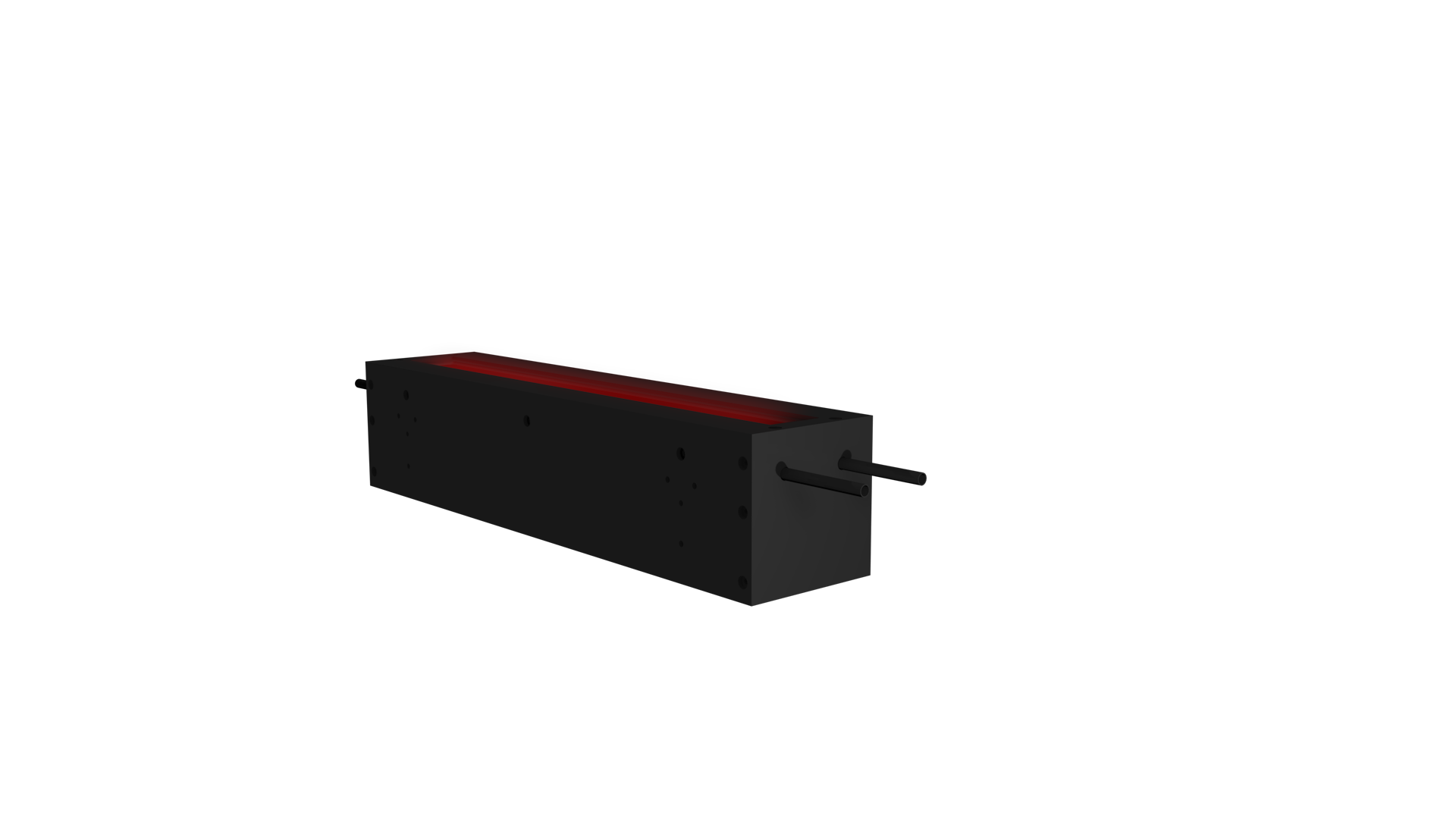
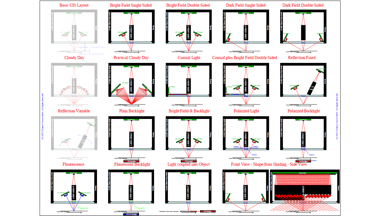
Inside the production
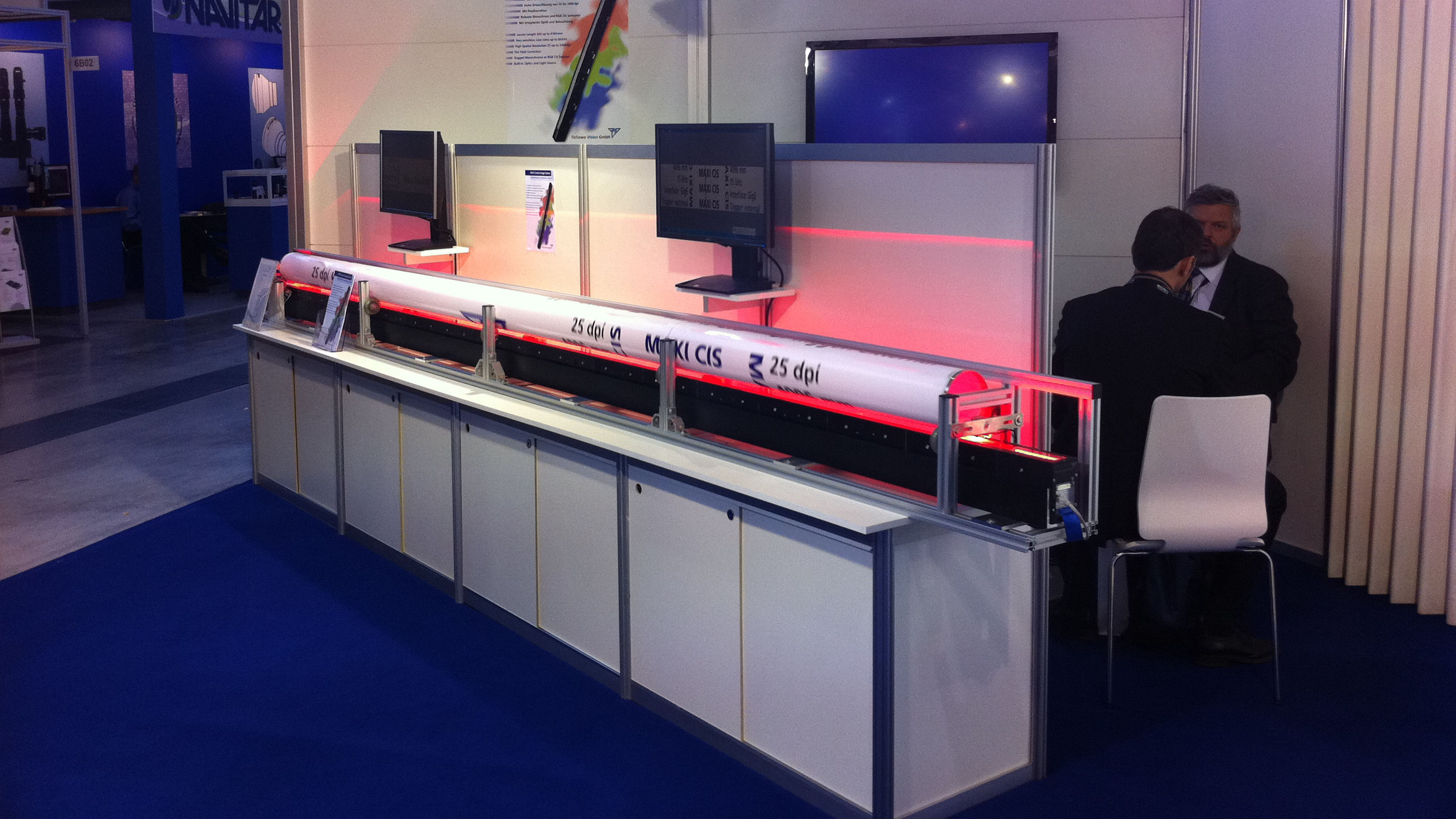
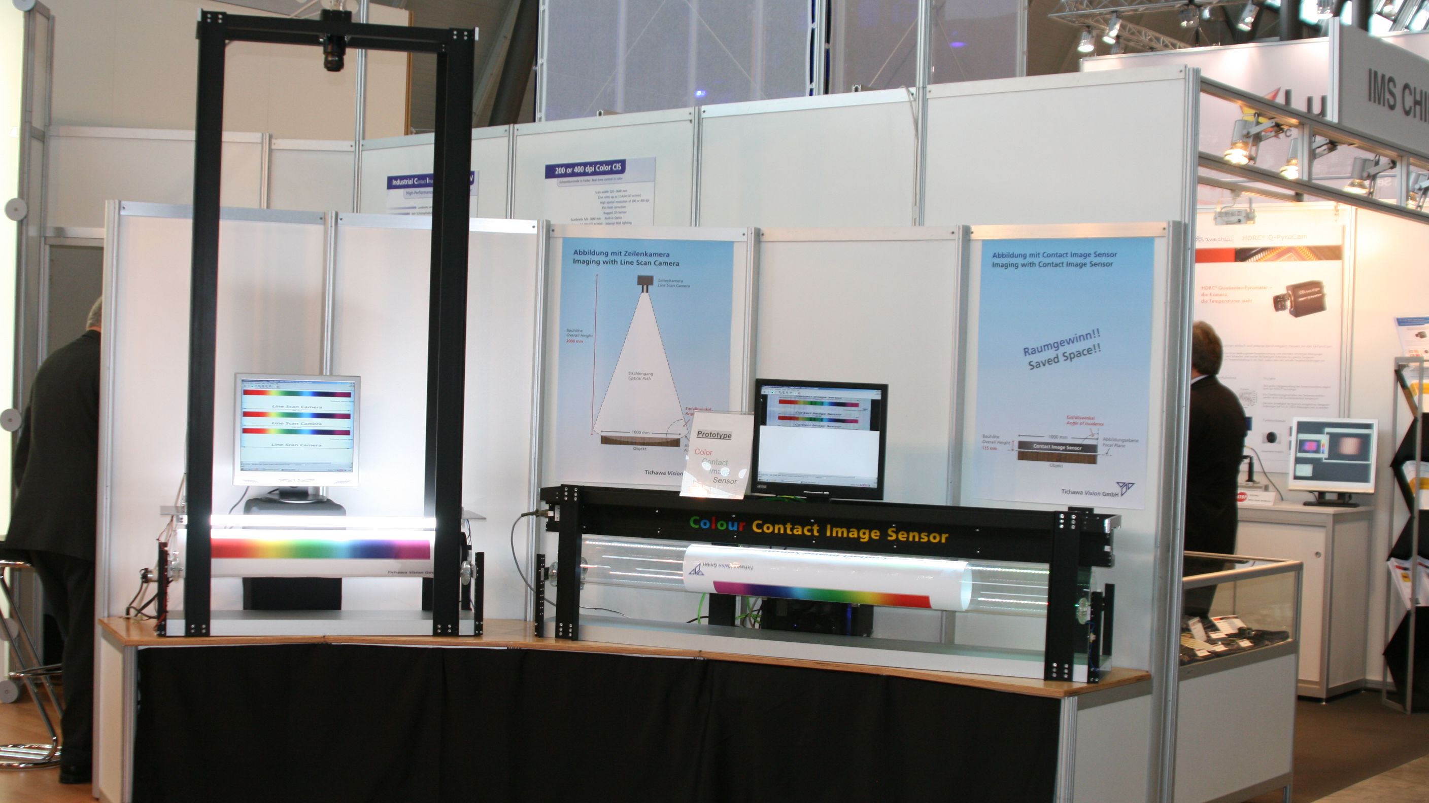
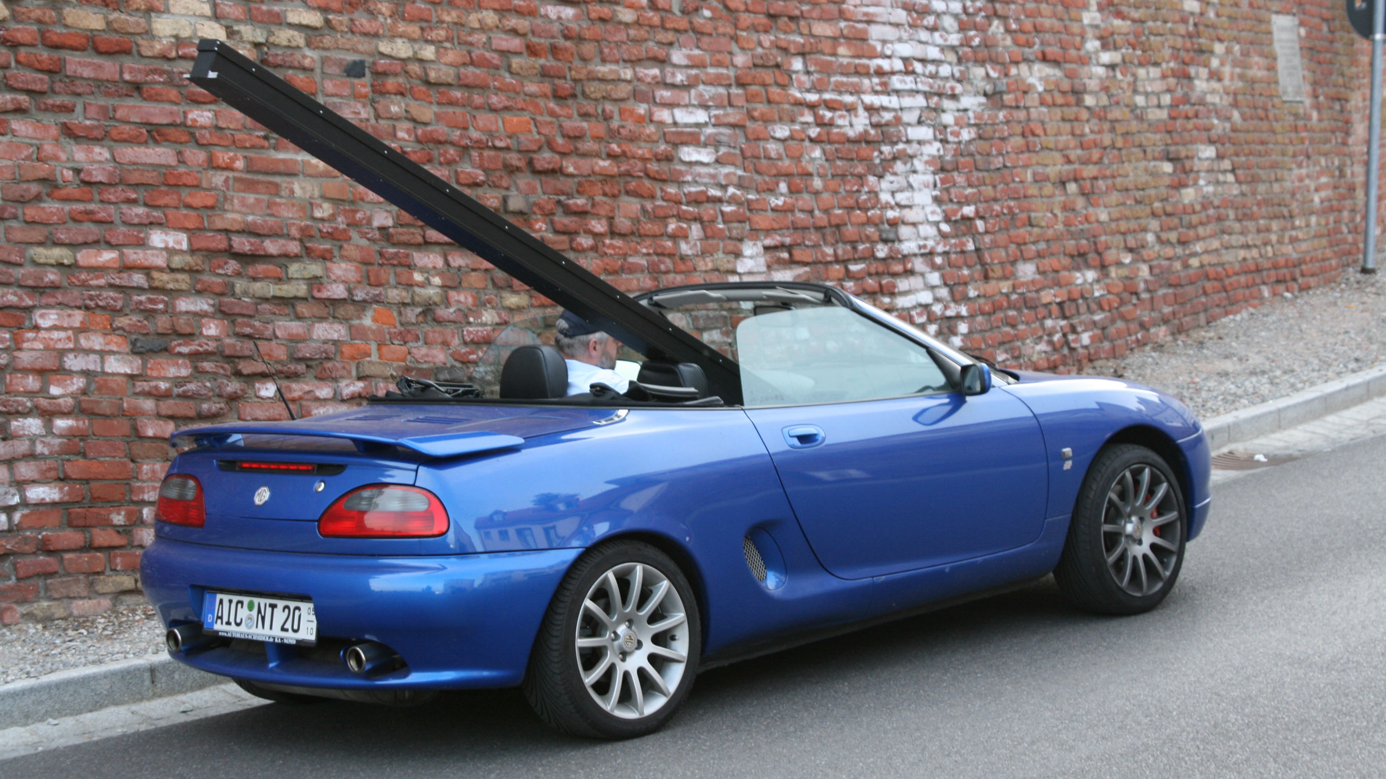
Industries
Processes & technical limits
| Processes | Tolerance | Max. part | Weight | Lot size | Materials |
|---|---|---|---|---|---|
| Development, manufacturing and distribution of optical and electronic components and devicesInspection | – | – | – | – | Silicon |
| Custom CIS solutions / modified standard products (Contact Image Sensors)Engineering | – | 4 m | – | – | – |
| CIS with resolutions from 25 dpi (pixel pitch 1.016 mm) to 2400 dpi (pixel pitch 10.6 μm),Inspection | – | 4 m | – | – | – |
| BDCIS - Basic Distance CIS (increased working distance, resolution up to 240 dpi as standard,Inspection | – | – | – | – | – |
| MXCIS - Maxi CIS (all-in-one: illumination, optics, sensors, data preprocessing; resolutions 100Inspection | – | 4 m | – | – | – |
| VUCIS - VARI Universal CIS (16 illumination geometries, 10 illumination colors, 8 optics withInspection | – | – | – | – | – |
Additional services
Reference customers
Quality
The management system of Tichawa Vision GmbH is certified to DIN EN ISO 9001:2015 by Intertek (initial certification in 2000). The scope covers the development, manufacturing and distribution of optical and electronic components and devices.
| Evidence | Friedberg |
|---|---|
| ISO 9001 |
History
- 1991
Founding of the Tichawa engineering office
- 1997
Founding of Tichawa Vision GmbH
- 2000
Initial certification to ISO 9001 on 29 August
- 2001
Krisztina Tichawa becomes managing director of Tichawa Vision GmbH
- 2011
Founding/management of Tichawa IP GmbH by Krisztina Tichawa