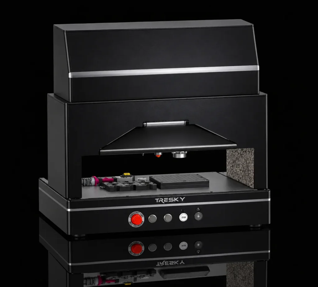
Develops, produces and distributes high-precision DIE Bonders for the semiconductor and photonics industries.

Tresky GmbH
Hennigsdorf (DE) · Taipei (TW) · Morganville, NJ (USA)New on Amplifa
About Tresky
Tresky GmbH, headquartered in Hennigsdorf near Berlin, develops, produces and distributes high-precision placement systems (DIE Bonders) for research, development and series production in the semiconductor industry. The modular systems cover all common DIE bonding processes: epoxy and UV bonding, ultrasonic, thermocompression, eutectic, flip chip and 3D bonding as well as sintering and photonics bonding with active alignment. The machines are manufactured at the Hennigsdorf site and can be individually tailored to the production requirements of international customers. In addition, the company offers contract manufacturing for prototypes and small series in assembly and interconnection technology at its own Contract Manufacturing Hub, including DIE sorting up to 12-inch wafers and packaging. Customer industries include semiconductor and microelectronics, power electronics/e-mobility, photonics, MedTech as well as research and development. With locations in Germany, Taiwan and the USA and a worldwide sales and service network, Tresky serves customers around the globe.
- Site
- Hennigsdorf
- Processes
- Epoxy/Adhesive DIE Bonding, UV Bonding, Ultrasonic Bonding (US Bonding), Thermocompression Bonding (TC Bonding), Eutectic Bonding, Sintering (metal sintering, pre-sinter/wet-sinter), Large Area Sintering (half-bridge modules), Sintering with DIE Transfer Film process (DTF)
- Materials
- Epoxy adhesive (Epoxy), UV adhesive, Silver sinter paste, Copper sinter paste, DIE Transfer Film (DTF), Gold, Indium, Gold-tin alloy
- Certificates
- On-site maintenance and remote maintenance
- Founded
- 1980
- Employees
- 25
- Industries
- Semiconductor industry, Power electronics/e-mobility, Photonics/Optoelectronics, Microelectronics, Defense/Security, MedTech
- 01
Consulting and process development
- 02
Design and engineering
- 03
Machine building in Hennigsdorf
- 04
Contract manufacturing (Contract Manufacturing Hub)
- 05
Sales and installation
- 06
Maintenance, on-site service and remote maintenance
Processes and Materials
Epoxy adhesive (Epoxy)
Widely used adhesive for conductive or insulating chip-substrate connections in epoxy bonding.
UV adhesive
Cures only under UV irradiation, suitable for temperature-sensitive chips and inline processes.
Silver sinter paste
High-temperature-resistant, thermomechanically stable connection for power semiconductors such as SiC MOSFETs and IGBTs.
Copper sinter paste
Alternative sinter paste for power electronics assemblies with high thermal resilience.
DIE Transfer Film (DTF)
Transfer film process for applying silver sinter layers over large areas onto DBC and AMB substrates.
Gold (Au)
Bump and joint material for thermocompression and ultrasonic bonding processes.
Indium (In)
Soft joint material for TC bonding processes for RF and optoelectronic devices.
Gold-tin alloy
Eutectic alloy for robust, temperature-stable chip connections.
Gold-silicon alloy
Eutectic bonding material for chip-substrate connections in the eutectic bonder.
SiC MOSFET, IGBT, GaN HEMT
Power semiconductors that are joined in the sintering process onto DBC and AMB substrates.
Locations
Hennigsdorf
DEHeadquarters: development, production, sales, Contract Manufacturing Hub
- Lot size
- Prototypes to small series
- Materials
- Semiconductor chips, sinter pastes, adhesives
- Epoxy Bonder
- UV Bonder
- Ultrasonic Bonder
- Thermocompression Bonder
- Sinter Bonder
- Flip Chip Bonder
- Eutectic Bonder
- 3D Bonder
- Photonics Bonder T-7000
- Lab Bonder T-200
Taipei
TWTresky Asia – Sales and sales support for Asia
Morganville (NJ)
USATresky Corp. (US) – Service and sales for North America
Systems and Applications
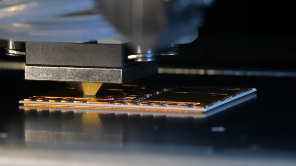
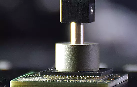
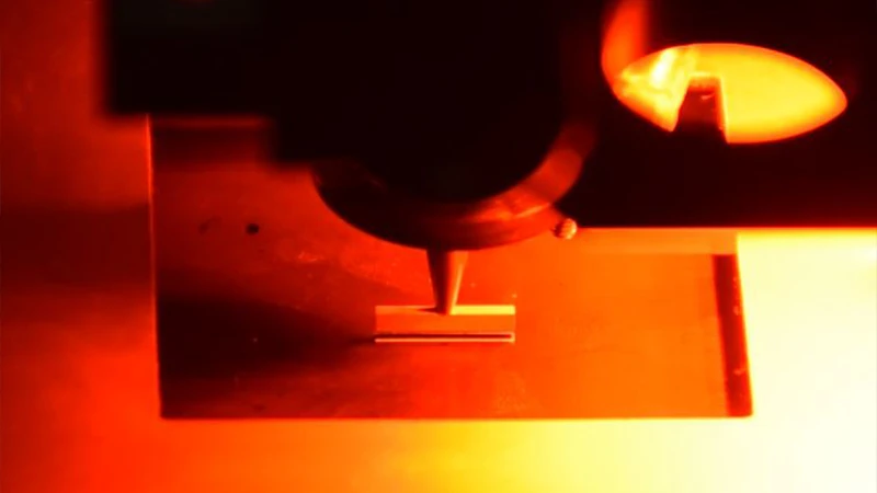
Inside the production

Industries
Processes & technical limits
| Processes | Tolerance | Max. part | Weight | Lot size | Materials |
|---|---|---|---|---|---|
| Epoxy/Adhesive DIE BondingJoining | – | – | – | – | Epoxy adhesive, Conductive adhesive |
| UV BondingJoining | – | – | – | – | UV adhesive |
| Ultrasonic Bonding (US Bonding)Joining | – | – | – | – | Gold (gold bumps), Semiconductor chips |
| Thermocompression Bonding (TC Bonding)Joining | – | – | – | – | Gold, Indium, Au-Au, Au-Si |
| Eutectic BondingJoining | – | – | – | – | AuSn 80/20, AuSi |
| Sintering (metal sintering, pre-sinter/wet-sinter)Joining | – | – | – | – | Silver sinter paste, Copper sinter paste, DIE Transfer Film (DTF), SiC MOSFET, IGBT, GaN HEMT |
| Large Area Sintering (half-bridge modules)Joining | – | – | – | – | Silver sinter paste, AMB substrates, SiC MOSFET |
| Sintering with DIE Transfer Film process (DTF)Joining | – | – | – | – | Silver sinter layer (transfer film), DBC substrates, AMB substrates |
| Flip Chip BondingJoining | – | – | – | – | Gold (bumps), Solder joints |
| 3D Bonding (DIE Stacking)Joining | – | – | – | – | Semiconductor chips, MEMS, Sensors, Logic chips |
| Photonics BondingJoining | – | – | – | – | Laser diodes, Photodiodes, Optoelectronic components |
| Active Alignment for Photonics SystemsAssembly | Nanometer precision | – | – | – | Fibers, Chips, Lenses, Laser diodes |
| DIE Sorting up to 12" wafers, Pick & Place and PackagingAssembly | – | 12" wafer | – | – | Semiconductor DIEs |
| Contract Manufacturing: Prototyping and small series in assembly and interconnection technologyJoining | – | – | – | – | Semiconductor chips |
10 Anlagen & Maschinen
| Machine | Manufacturer / model | Quantity | Working area | Year built | Site |
|---|---|---|---|---|---|
| Epoxy Bonder | Tresky | – | – | – | Hennigsdorf |
| UV Bonder | Tresky | – | – | – | Hennigsdorf |
| Ultrasonic Bonder | Tresky | – | – | – | Hennigsdorf |
| Thermocompression Bonder | Tresky | – | – | – | Hennigsdorf |
| Sinter Bonder | Tresky | – | – | – | Hennigsdorf |
| Flip Chip Bonder | Tresky | – | – | – | Hennigsdorf |
| Eutectic Bonder | Tresky | – | – | – | Hennigsdorf |
| 3D Bonder | Tresky | – | – | – | Hennigsdorf |
| Photonics Bonder | Tresky T-7000 | – | – | – | Hennigsdorf |
| Lab Bonder | Tresky T-200 | – | – | – | Hennigsdorf |
Additional services
Quality
The systems are tailored to customer requirements; a worldwide network of technicians at three locations and representatives ensures fast support, on-site maintenance and remote maintenance.
| Evidence | Hennigsdorf | Taipei | Morganville (NJ) |
|---|---|---|---|
| On-site maintenance and remote maintenance |
History
- 1980
Company founded; 40 years of experience in the semiconductor market.
- 2017
Company split; afterwards growth from 6 to currently 25 employees.