Customized VCSELs, VCSEL arrays, LEDs and photodiodes – with cleanroom, assembly and test in Ulm.

Vertical Photonics GmbH
UlmNew on Amplifa
Photonics engineering from device physics to packaging
Vertical Photonics is a photonics engineering service provider based in Science Park II in Ulm. The company develops and manufactures customized VCSELs and VCSEL arrays, LEDs (visible and NIR) and high-speed photodiodes with spectral coverage from UV to IR. The service portfolio covers the entire stack: device and mask design, custom epitaxial structure design, rapid prototyping, small-volume production, cleanroom services (metal contacts, etching, passivation, wet oxidation, grinding/polishing, dicing), chip-on-board assembly with eutectic and epoxy die attach as well as Au/Al wire and ribbon bonding and flip-chip, packaging in TO cans, on ceramic submounts and in custom housings, and wafer and die test with L-I-V, spectral and beam-profile measurements. Customer industries include data communications, sensing & LiDAR, medical & life sciences, industrial metrology, consumer electronics and defense & aerospace. The target group ranges from research groups that need individual custom devices to OEMs requiring repeatable supply of packaged emitters. Manufacturing takes place in small series with process lock, SPC, reliability stress and full lot traceability.
- Site
- Ulm
- Processes
- VCSEL manufacturing (customized single- & multi-mode VCSELs, VCSEL arrays), LED manufacturing (visible & NIR LEDs), Photodiode manufacturing (UV to IR, high bandwidth), Consultancy & advisory (device & package architecture, epi design), Rapid prototyping (short-loop fab & test, L-I-V, spectral, beam profile), Small-volume production (process lock, SPC, lot traceability), Eutectic & epoxy die attach, Au & Al wire bonding, ribbon bonding
- Materials
- Gold (bond wire), Aluminum (bond wire), Ceramic (submounts), Epoxy (die attach), Eutectic solder material, VCSEL/LED/photodiode semiconductors (III-V compound semiconductors, implicit), Gold, Aluminum
- Certificates
- Lot traceability & SPC, Reliability stress testing, ISO 9001
- Industries
- Data Communications, Sensing & LiDAR, Medical & Life Sciences, Industrial Metrology, Consumer Electronics, Defense & Aerospace
- 01
Consulting & specification
- 02
Device and epi design / simulation
- 03
Short-loop fabrication (cleanroom)
- 04
Chip-on-board assembly (die attach, bonding, flip-chip)
- 05
Packaging
- 06
Wafer and die test / characterization
- 07
Small-volume production with qualification
Materials and processes
Gold
Bond wire and ribbon bonding for photonic chip interconnects.
Aluminum
Bond wire material for chip-on-board assembly.
Eutectic solder material
Die attach with thermally and electrically conductive connection.
Epoxy
Die attach material for assembly processes.
Ceramic
Submount material for packaging.
III-V semiconductors (VCSEL/LED/photodiode)
Base material of the manufactured photonic devices.
Sites
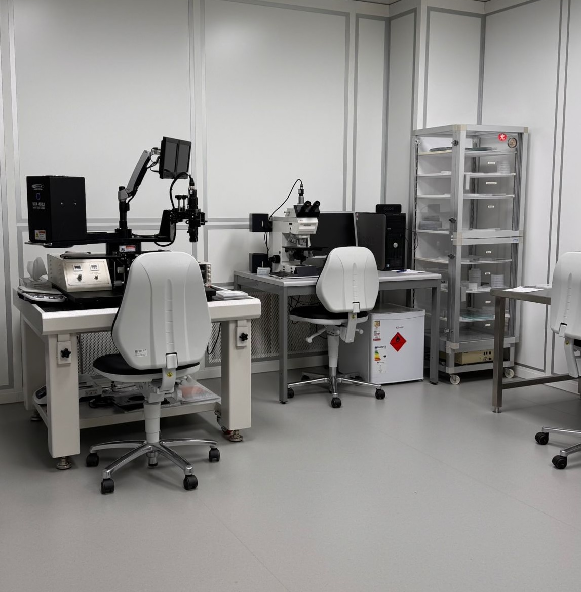
Ulm
DEHeadquarters with cleanroom, assembly & test
- Lot size
- Prototype to small series
- Materials
- III-V semiconductors, gold, aluminum, ceramic, epoxy, eutectic solder
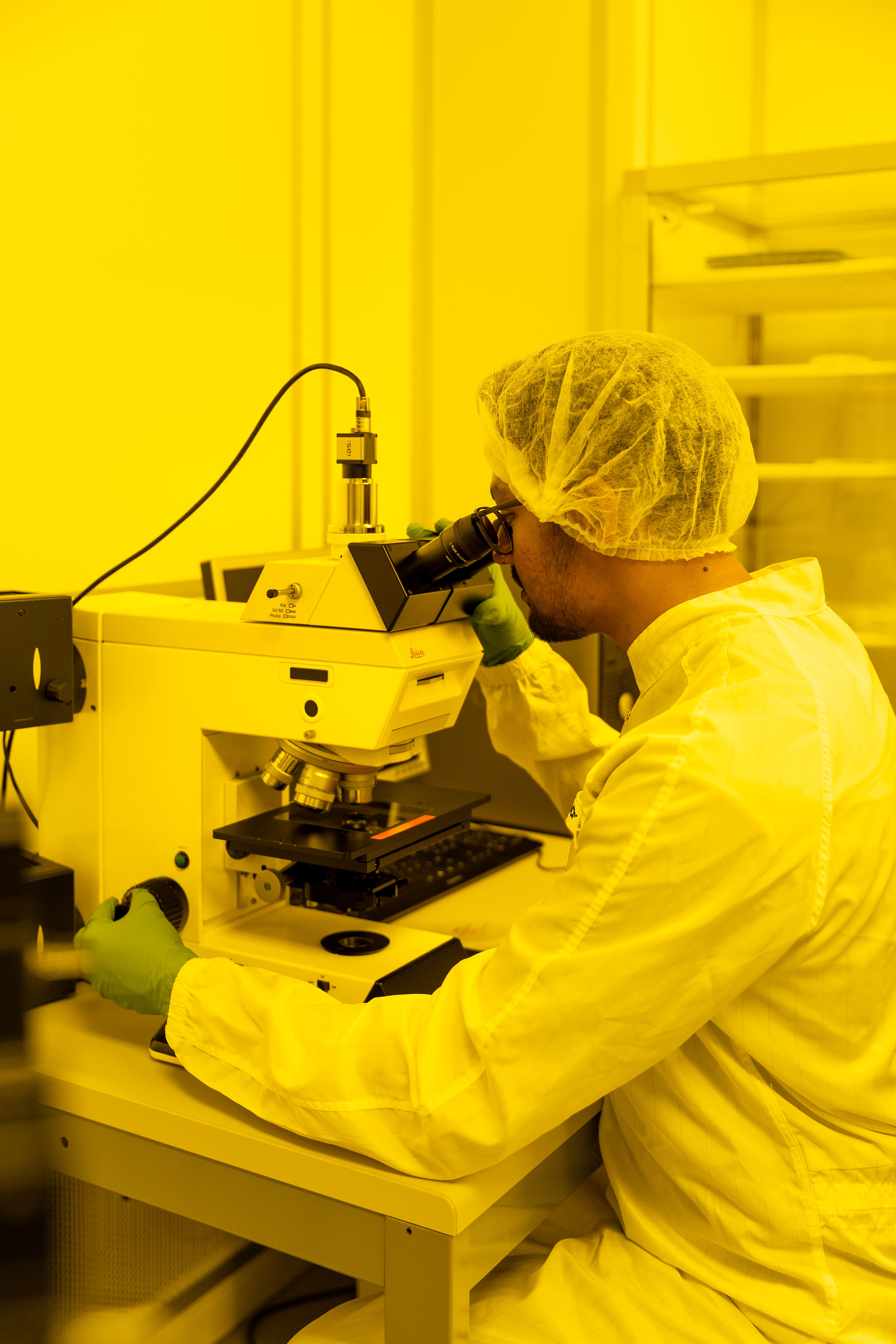
- Cleanroom
- Lithography / mask alignment
- Metal evaporation system
- Wet bench
- Dicing equipment
- Wire bonder / die attach
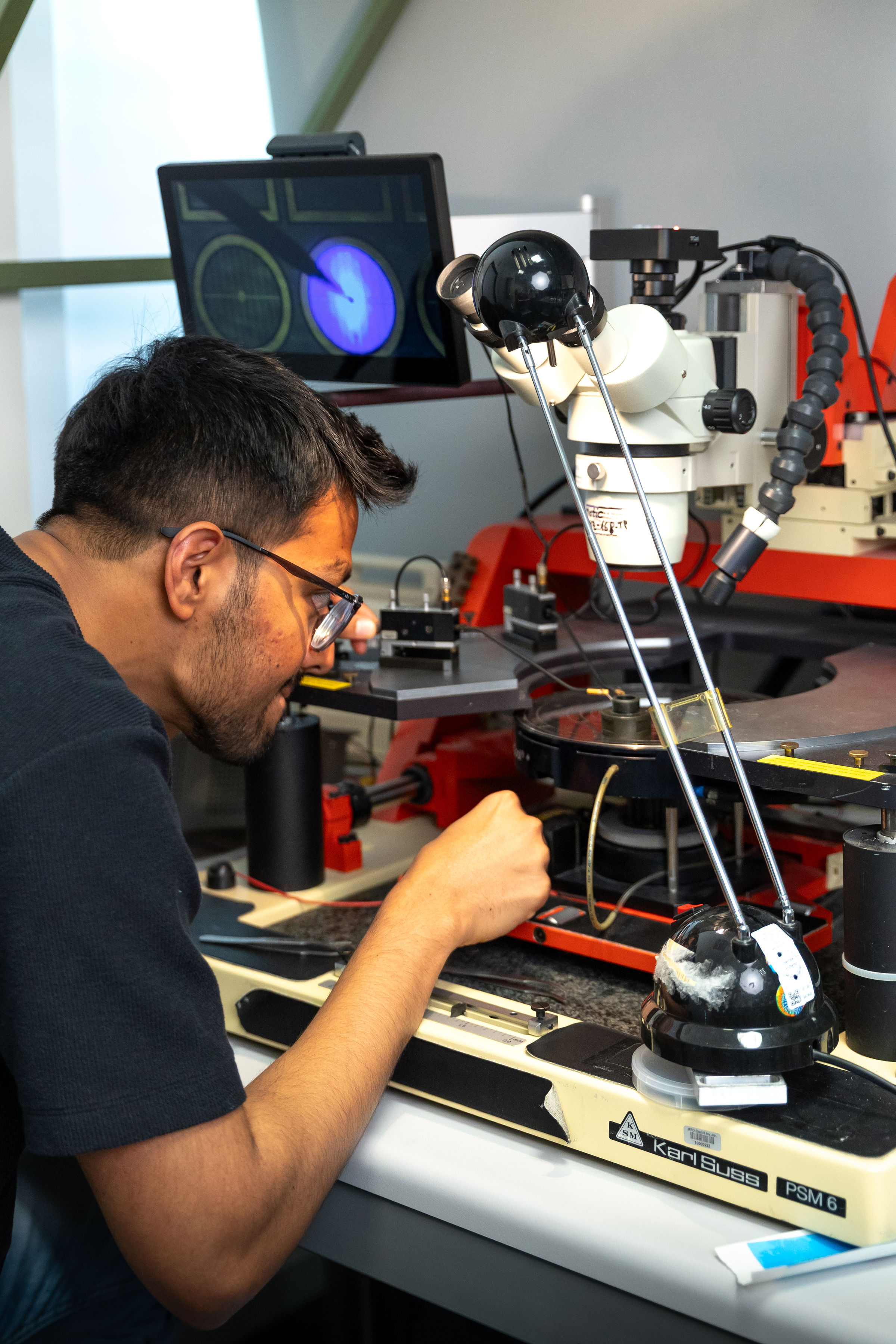
- Probe station
- Automated die tester & tape sorter
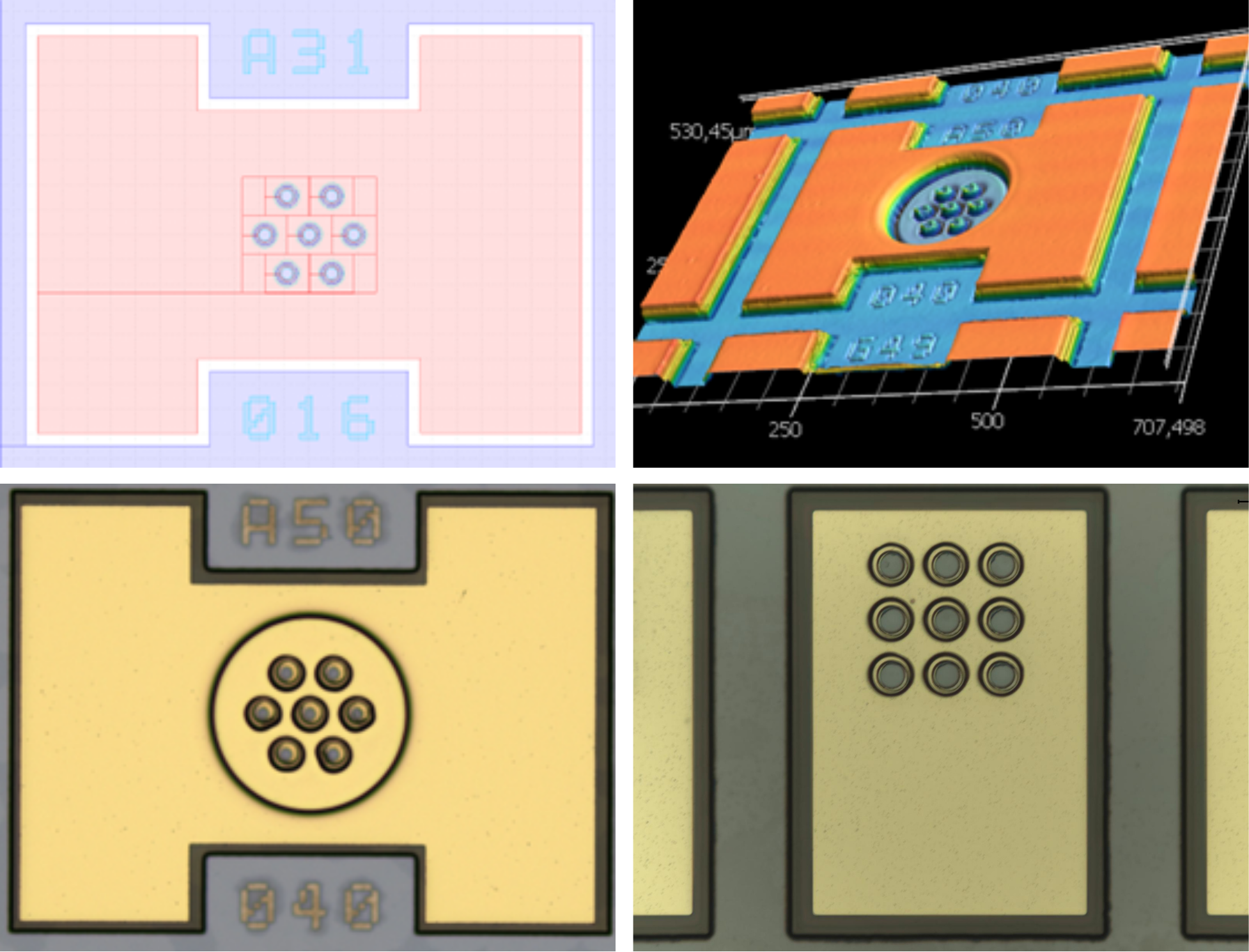
- 3D profile measurement system
Components
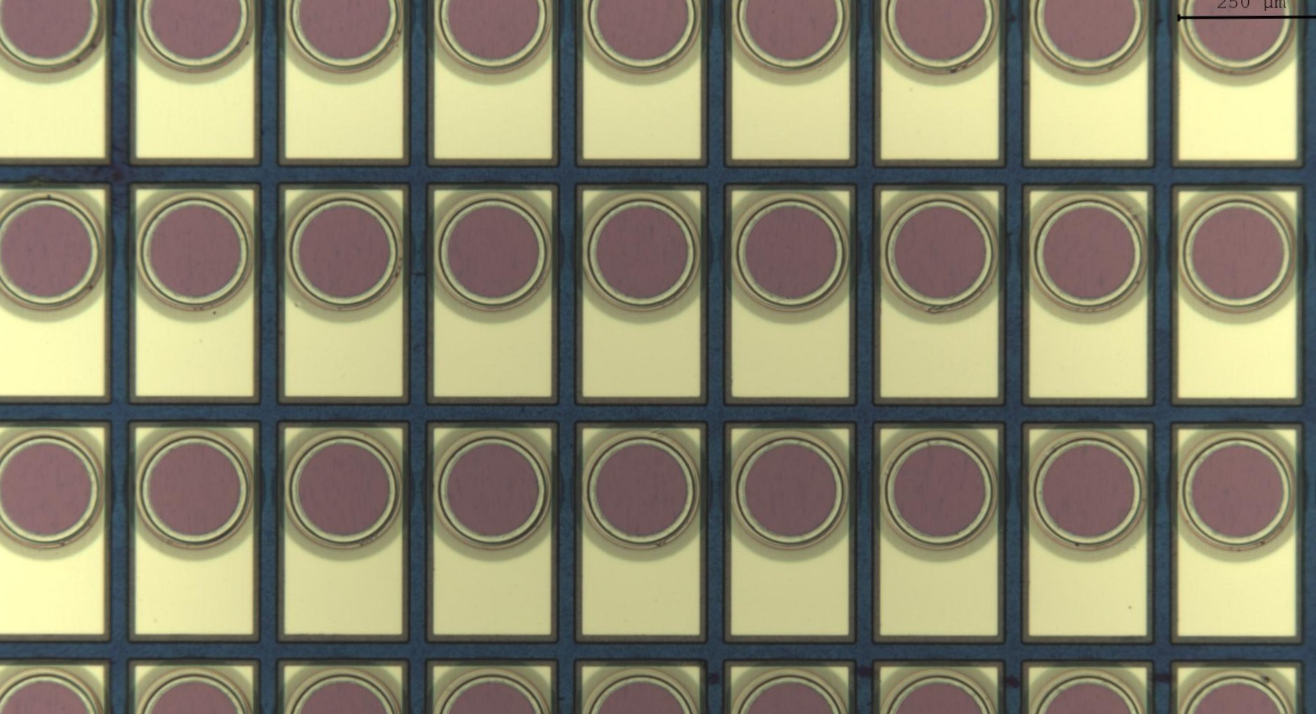
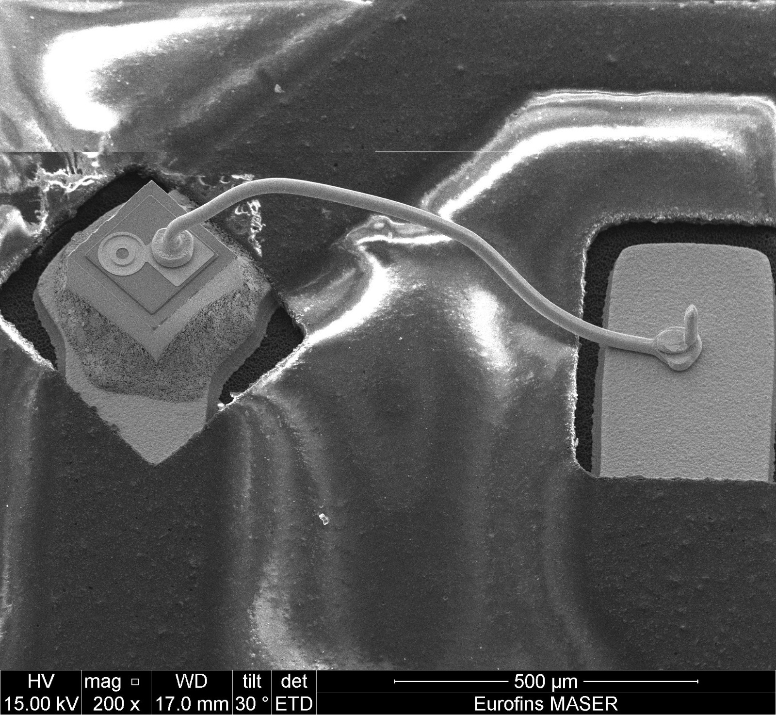
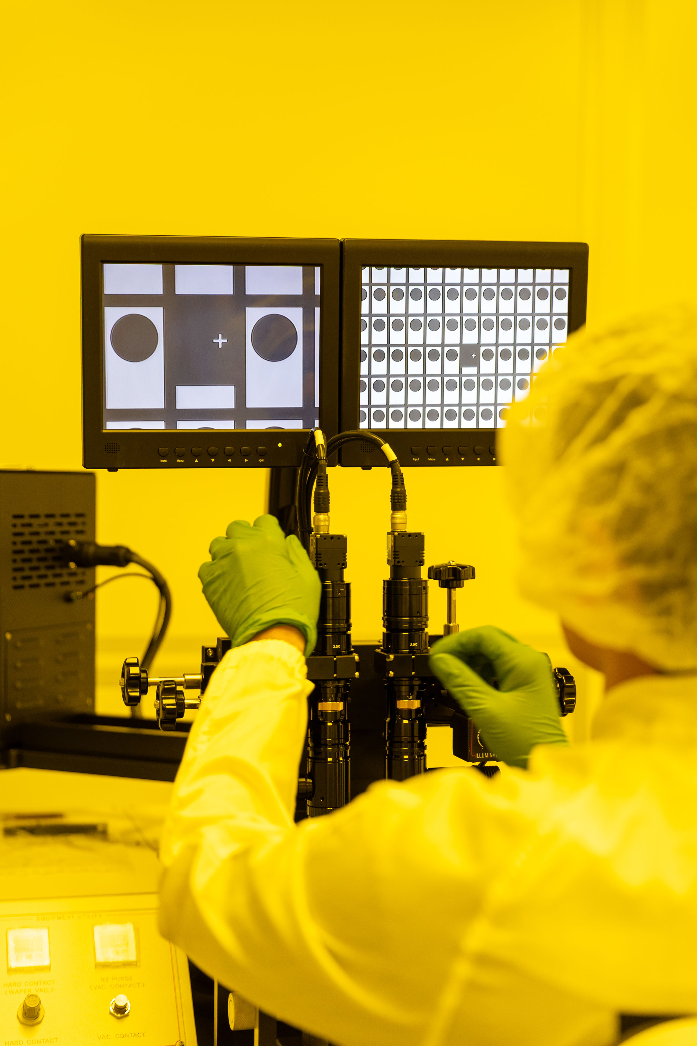
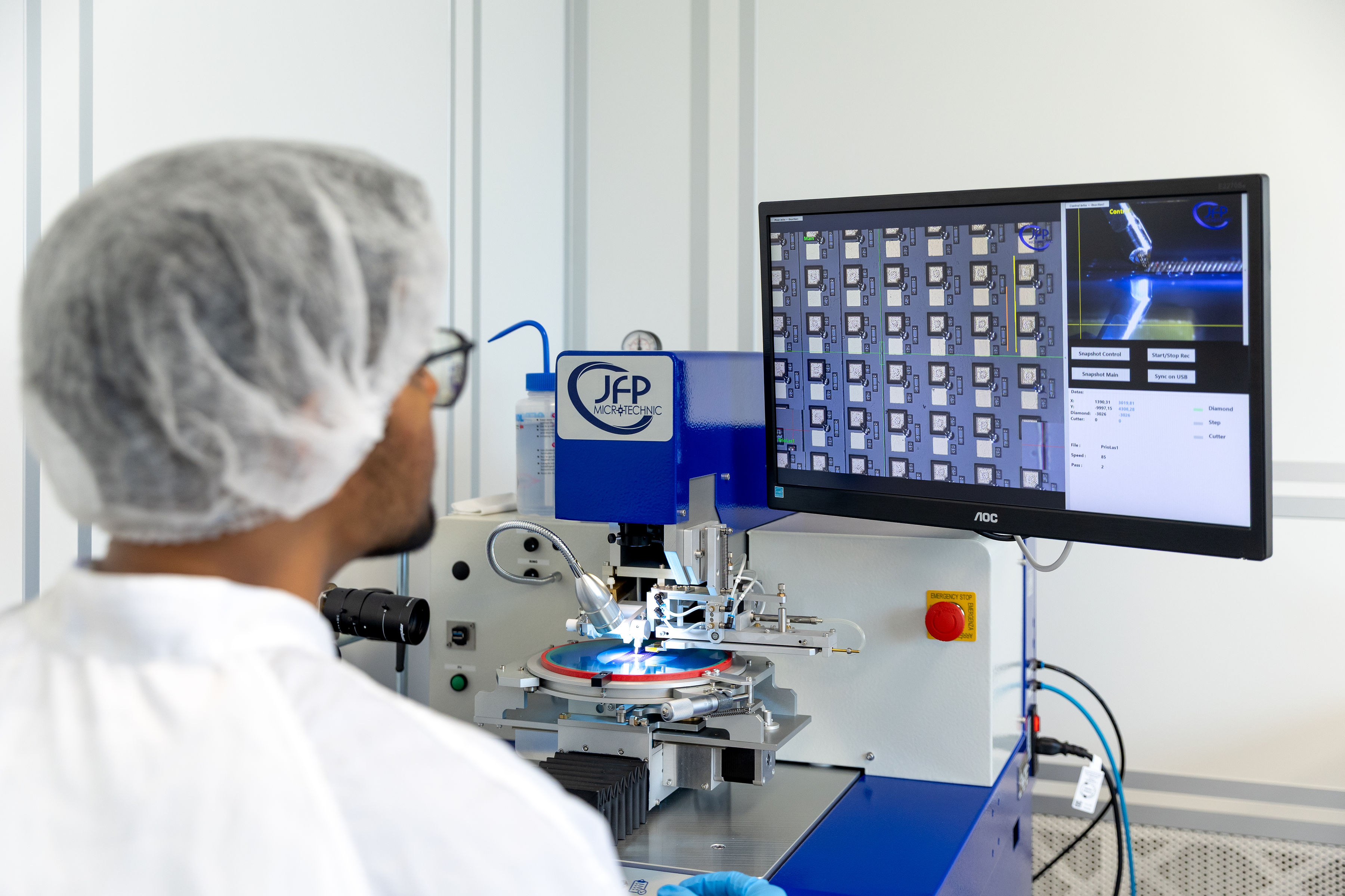
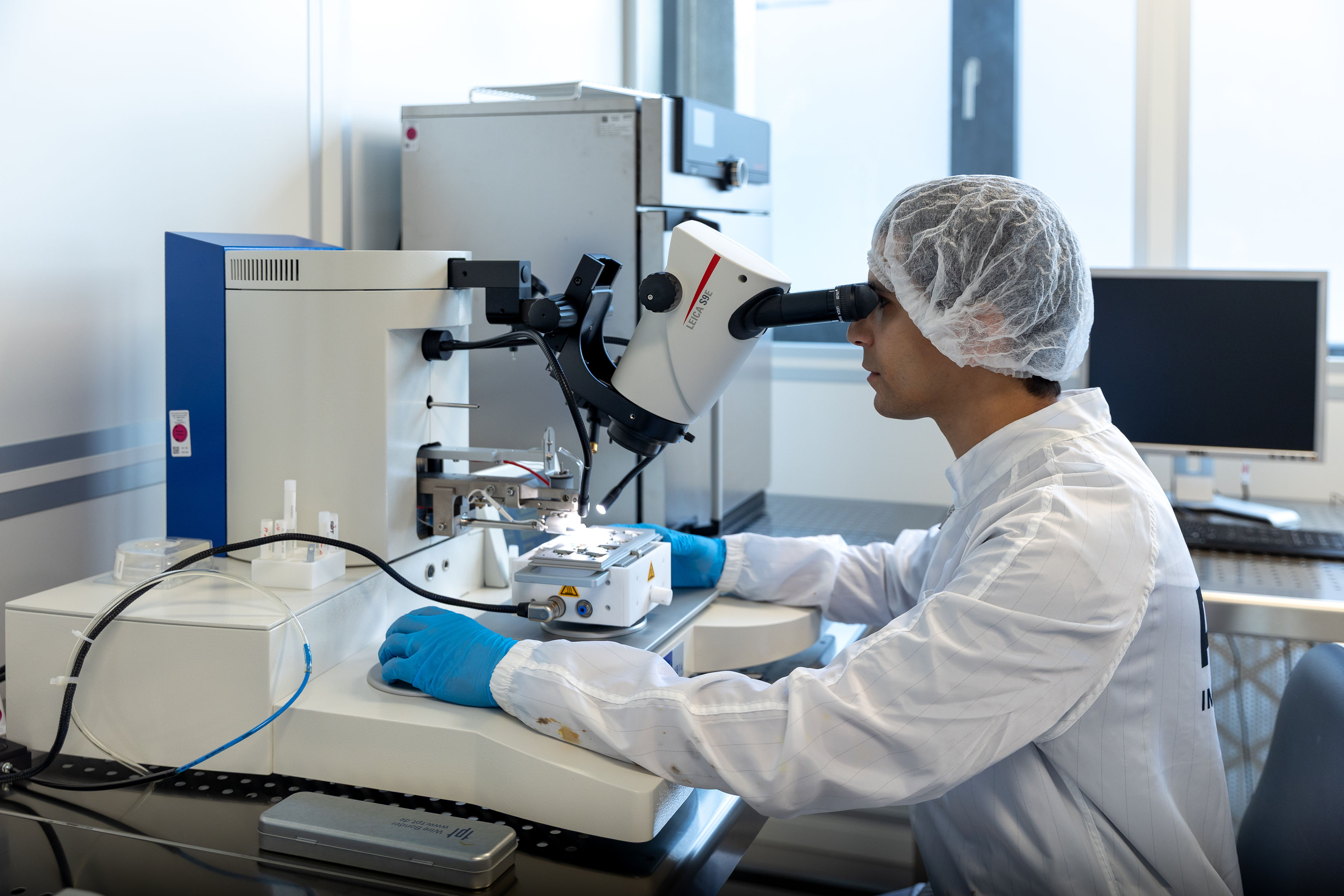
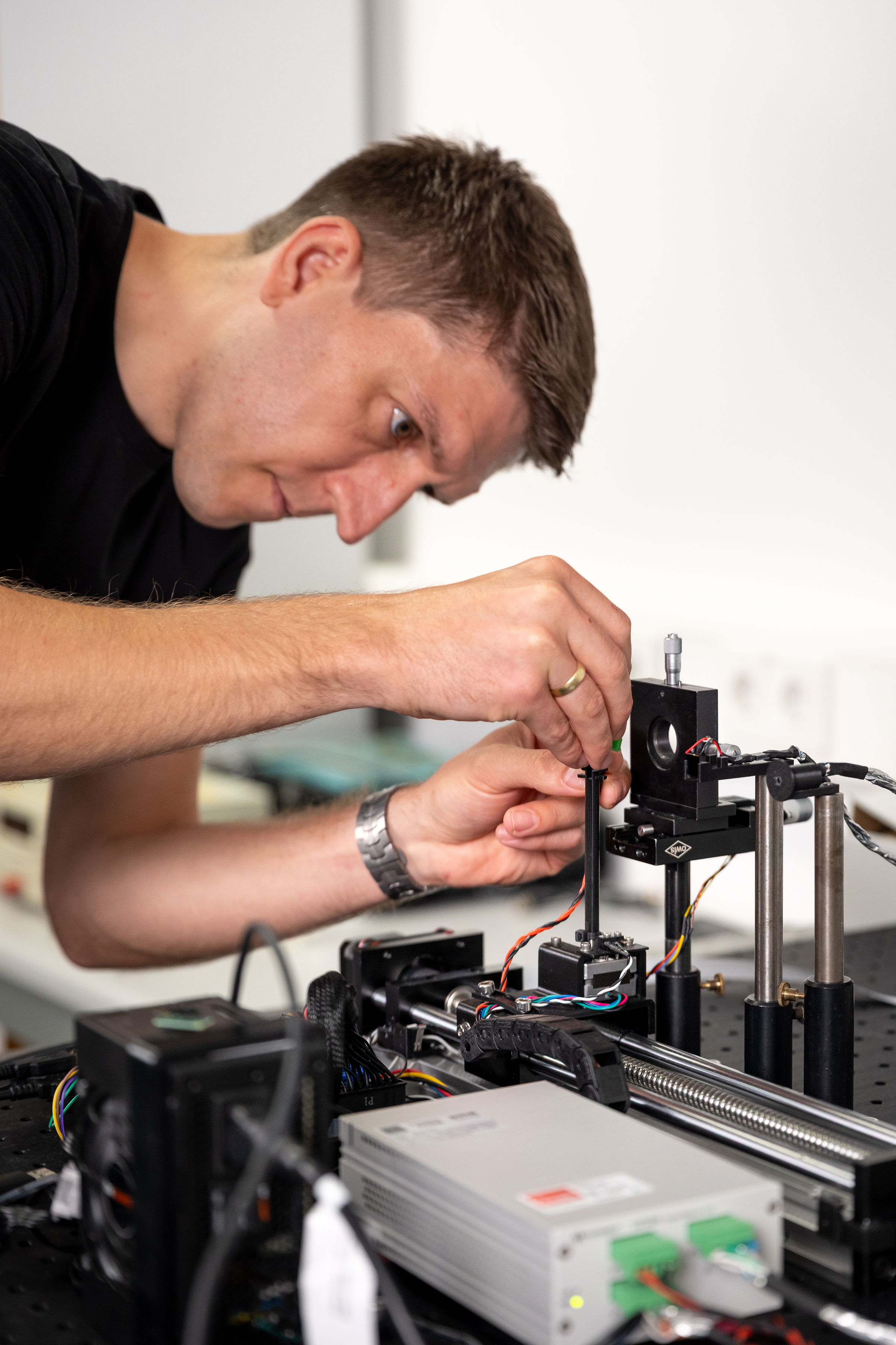
Inside the production
Industries
Processes & technical limits
| Processes | Tolerance | Max. part | Weight | Lot size | Materials |
|---|---|---|---|---|---|
| VCSEL manufacturing (customized single- & multi-mode VCSELs, VCSEL arrays)Semiconductor/Photonics (manufacture of photonic components) | – | – | – | Small-volume production | GaAs-based semiconductors (implicit, VCSEL) |
| LED manufacturing (visible & NIR LEDs)Semiconductor/Photonics | – | – | – | – | Semiconductors |
| Photodiode manufacturing (UV to IR, high bandwidth)Semiconductor/Photonics | – | – | – | – | Semiconductors |
| Consultancy & advisory (device & package architecture, epi design)Engineering | – | – | – | – | – |
| Rapid prototyping (short-loop fab & test, L-I-V, spectral, beam profile)Engineering | – | – | – | – | – |
| Small-volume production (process lock, SPC, lot traceability)Semiconductor/Photonics | – | – | – | – | – |
| Eutectic & epoxy die attachJoining | – | – | – | – | Semiconductor chips |
| Au & Al wire bonding, ribbon bondingJoining | – | – | – | – | Gold, Aluminum |
| Flip-chip assemblyJoining | – | – | – | – | Semiconductor chips |
| Hermetic & non-hermetic packaging (TO cans, ceramic submounts, custom housings)Assembly | – | – | – | small-series production | Ceramic, Metal |
| Metal contacts / metal evaporationSurface | – | – | – | – | Metals |
| EtchingSemiconductor process technology | – | – | – | – | – |
| PassivationSemiconductor process technology | – | – | – | – | – |
| Wet thermal oxidationSemiconductor process technology | – | – | – | – | – |
| Grinding & polishingSurface | – | – | – | – | – |
| Dicing & wafer singulationSemiconductor process technology | – | – | – | – | – |
| Lithography — multi-layer mask alignmentSemiconductor process technology | – | – | – | – | – |
| Wet bench processingSemiconductor process technology | – | – | – | – | – |
| Custom epitaxial structure designEngineering | – | – | – | – | – |
| Device & mask design (custom LED & VCSEL layouts)Engineering | – | – | – | – | – |
| Wafer & die test (probe-station characterization, automated L-I-V, spectral, beam profile)Testing | – | – | – | – | – |
| Electrical characterizationTesting | – | – | – | – | – |
| Optical characterizationTesting | – | – | – | – | – |
| Automated die testing & tape sortingTesting | – | – | – | – | – |
| Microscope inspectionTesting | – | – | – | – | – |
| 3D profile measurementsTesting | – | – | – | – | – |
| Cleanroom services (full photonics device processing stack)Semiconductor process technology | – | – | – | – | – |
| Collaborative engineering & co-developmentEngineering | – | – | – | – | – |
9 Anlagen & Maschinen
| Machine | Manufacturer / model | Quantity | Working area | Year built | Site |
|---|---|---|---|---|---|
| Cleanroom (controlled-environment processing) | – | – | – | – | Ulm |
| Probe station (wafer/die test) | – | – | – | – | Ulm |
| Lithography / mask alignment system | – | – | – | – | Ulm |
| Metal evaporation system | – | – | – | – | Ulm |
| Wet bench | – | – | – | – | Ulm |
| Dicing equipment (wafer singulation) | – | – | – | – | Ulm |
| Wire bonder / die attach equipment | – | – | – | – | Ulm |
| 3D profile measurement system | – | – | – | – | Ulm |
| Automated die tester & tape sorter | – | – | – | – | Ulm |
Additional services
Quality and traceability
Every device is characterized and documented – with L-I-V curves, spectra, reliability stress and complete lot documentation. Small-volume production includes process lock, qualification, SPC and full lot traceability at the quality level of high-volume manufacturing.
| Evidence | Ulm |
|---|---|
| Lot traceability & SPC | |
| Reliability stress testing | |
| ISO 9001 |