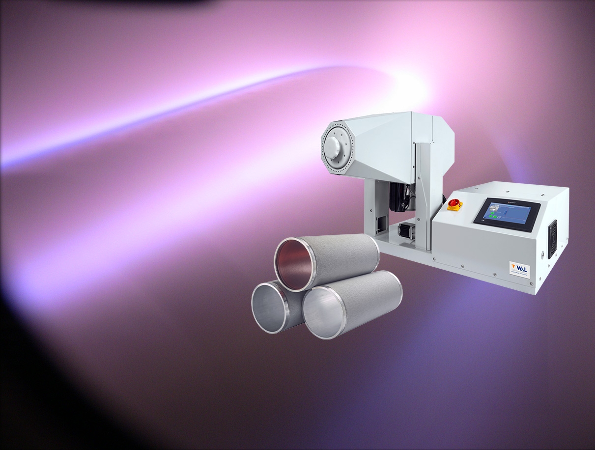
Process and system development for vacuum thin-film coating (PVD/PECVD) with a focus on diamond layers.

W&L-Coating Systems GmbH
Reichelsheim (Headquarters)New on Amplifa
About W&L-Coating Systems
W&L-Coating Systems GmbH is a specialized company based in Reichelsheim (Wetterau) and a subsidiary of Schneider Optical Machines. The company develops processes and production systems for vacuum-based functional coatings – metallic, ceramic and organic layers – on customer substrates, with a particular focus on carbon modifications such as polycrystalline diamond. Core processes are physical vapour deposition (PVD/magnetron sputtering) for extremely thin metallic and ceramic layers on large areas, as well as plasma-enhanced chemical vapour deposition (PECVD) with microwave excitation via linear, coaxial plasma source arrays that enable homogeneous discharges of 1,000 mm and more and areas up to the square-metre range. A central element is the upscaling of laboratory processes to production-ready systems, complemented by system design, cost-of-ownership consulting and characterization using XPS and FT-IR. In-house applications include boron-doped diamond electrodes for wastewater treatment and ozone generation as well as biocompatible diamond layers for implant surfaces.
- Site
- Reichelsheim
- Processes
- Physical Vapour Deposition (PVD), magnetron sputtering, Plasma Enhanced Chemical Vapour Deposition (PECVD) with microwave excitation, Thin-film coating of large areas (linear plasma sources, arrays), Diamond coating (polycrystalline, boron-doped, PECVD), Quartz coating from HMDSO/TEOS (rates up to 1 micrometer per second), Precious metal thin-film coating on low-cost substrates (PVD), Coating of implant surfaces with diamond layers, Boron-doped diamond electrode and cell technology for wastewater treatment/ozone generation
- Materials
- Diamond (polycrystalline, gridded, boron-doped), Quartz (SiO2), Organically modified ceramic (SiOC), HMDSO (hexamethyldisiloxane, precursor), TEOS (tetraethoxysilane, precursor), Precious metals (thin film), Metallic functional coatings, Ceramic functional coatings
- Industries
- Wastewater/environmental engineering, Medical technology (implants), Optics/mechanical engineering, Surface technology, Medical technology/implants, Optics/mechanical engineering (parent company Schneider Optical Machines)
- 01
Process development (PVD/PECVD)
- 02
System layout and system design
- 03
Upscaling from laboratory to production systems
- 04
Coating of customer substrates
- 05
Layer characterization (XPS, FT-IR)
Layer materials and processes
PVD / magnetron sputtering
Deposition of extremely thin, dense metallic and ceramic layers on large areas by plasma erosion of target material.
PECVD (microwave plasma)
Deposition of organic, ceramic and crystalline layers from liquid or gaseous precursors in a vacuum plasma.
Polycrystalline diamond
Diamond layers deposited by PECVD with controllable morphology, among other things for biocompatible implant surfaces.
Boron-doped diamond
Electrically conductive diamond layers for electrodes for wastewater treatment and ozone generation in aqueous environments.
Quartz (SiO2)
Hard, scratch-resistant quartz layers deposited from HMDSO or TEOS at rates of up to 1 µm per second.
Organically modified ceramic (SiOC)
Flexible, scratch-resistant quartz layers with low carbon content under oxygen deficiency in the plasma.
Hexamethyldisiloxane (precursor)
Liquid precursor that is oxidatively deposited as quartz layers in an oxygen plasma.
Tetraethoxysilane (precursor)
Alternative silicon precursor for the deposition of quartz and ceramic layers.
Precious metal thin films
Precious metal layers deposited by PVD onto low-cost substrates, providing precious-metal surface properties without full-material costs.
Metallic and ceramic functional coatings
Functional layers on customer substrates using standardized or customized processes.
Locations
Reichelsheim
DEHeadquarters: process development, system engineering, coating, BDD electrode and cell technology
- Lot size
- Prototype to production (upscaling)
- Materials
- Diamond, boron-doped diamond, quartz (SiO2), SiOC, precious metals, metallic and ceramic functional layers
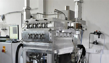
- NCS – Nano Crystalline System (large-area PECVD platform)
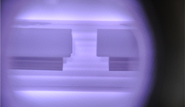
- Linear microwave plasma sources (coaxial plasma line arrays)
- Vacuum coating systems with load locks, valves and vacuum pumps
- XPS depth profile analysis
- FT-IR spectroscopy
Products and systems
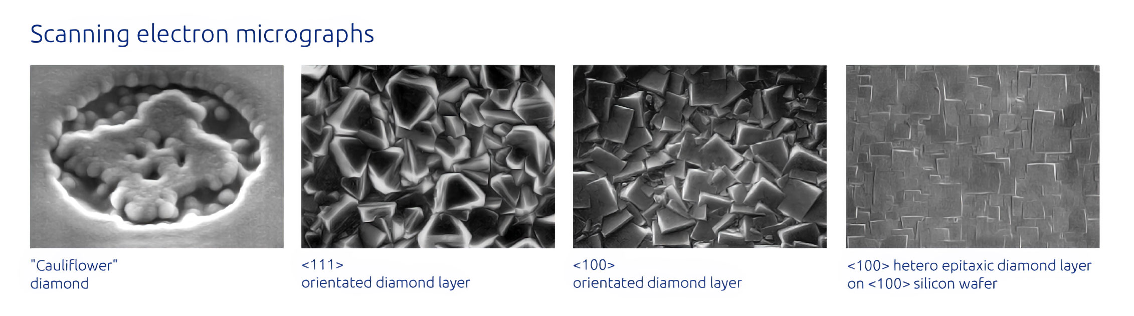
Inside the production
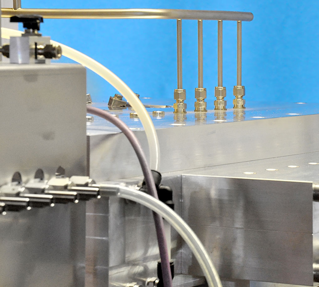
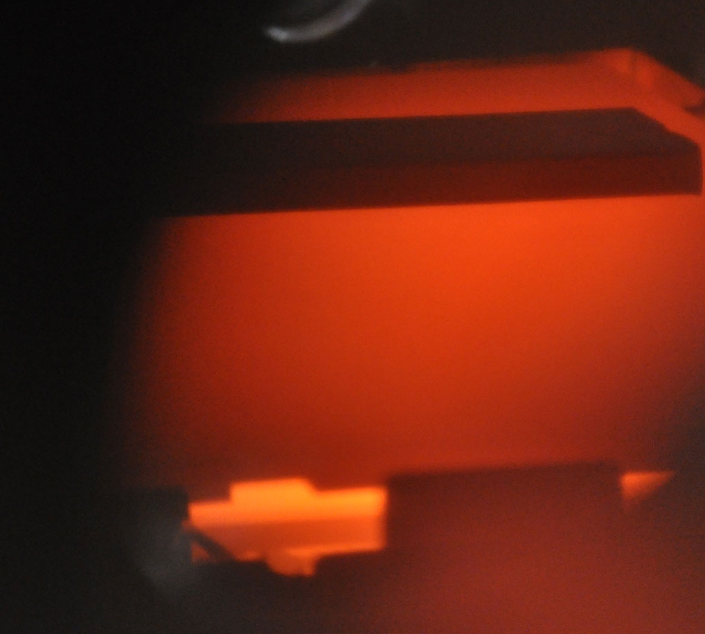


Industries
Processes & technical limits
| Processes | Tolerance | Max. part | Weight | Lot size | Materials |
|---|---|---|---|---|---|
| Physical Vapour Deposition (PVD), magnetron sputteringSurface | – | – | – | – | Metals, Ceramics |
| Plasma Enhanced Chemical Vapour Deposition (PECVD) with microwave excitationSurface | – | – | – | – | Organic, Ceramics, crystalline layers (diamond), organically modified ceramics |
| Thin-film coating of large areas (linear plasma sources, arrays)Surface | – | linear plasma beam 1,000 mm and more | – | – | nanocrystalline diamond, quartz (SiO2), organically modified ceramics |
| Diamond coating (polycrystalline, boron-doped, PECVD)Surface | – | – | – | – | diamond, boron-doped diamond |
| Quartz coating from HMDSO/TEOS (rates up to 1 micrometer per second)Surface | – | – | – | – | quartz (SiO2), organically modified ceramics |
| Precious metal thin-film coating on low-cost substrates (PVD)Surface | – | – | – | – | precious metals |
| Coating of implant surfaces with diamond layersSurface | – | – | – | – | diamond |
| Boron-doped diamond electrode and cell technology for wastewater treatment/ozone generationSurface | – | – | – | – | boron-doped diamond |
| Design/engineering of vacuum systems (vacuum coating systems, engineering)Engineering | – | – | – | – | – |
| Process development and upscaling from laboratory systems to production systems (PVD/PECVD)Engineering | – | – | – | – | – |
| Cost-of-ownership consulting for vacuum coating systemsEngineering | – | – | – | – | – |
| XPS depth profile analysis (characterization)Testing | – | – | – | – | – |
| FT-IR spectroscopy (layer characterization)Testing | – | – | – | – | – |
3 Anlagen & Maschinen
| Machine | Manufacturer / model | Quantity | Working area | Year built | Site |
|---|---|---|---|---|---|
| NCS – Nano Crystalline System (large-area PECVD platform) | W&L Coating Systems NCS | – | Aluminium frames and flanges with water cooling, process gas supply, plasma source array | – | Reichelsheim |
| Linear microwave plasma sources (coaxial plasma line arrays) | W&L Coating Systems (developed with University of Stuttgart) | – | linear discharges of 1,000 mm and more, areas up to the square-metre range | – | Reichelsheim |
| Vacuum coating systems with load locks, valves, vacuum pumps of all kinds | – | – | – | – | – |
Additional services