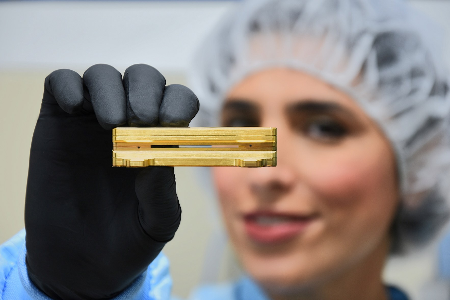
Specialized in flux-free vacuum soldering, packaging and thermal management for optical and photonic components

XCCES GmbH (PHOTONICPARTS)
Herzogenrath (Ericsson-Allee 1, NRW)New on Amplifa
About PHOTONICPARTS
PHOTONICPARTS is the brand of XCCES GmbH, founded in August 2023 by Dr. Jan Dolkemeyer and Phillip Dittmann in Herzogenrath. The company works in the field of joining and assembly technologies as well as the manufacturing of laser components for the photonic market. Its core competence is the production of homogeneous large-area solder joints for any materials and material combinations with low thermal and electrical resistance. Services include PVD deposition of solder layers (10–500 µm), solderable metallization via magnetron sputtering, flux-free vacuum soldering as a contract manufacturing service, active alignment in liquid solder, hermetic sealing technologies, as well as mechanical design and thermal simulation. Products manufactured include laser crystal packages (Cube, Slab, Rod), housings for non-linear crystals, mirror mounts and custom packages with soldered TECs. Materials include glass, metal, ceramics, optical components and laser crystals. Target markets are laser technology, photonics, quantum technologies and aerospace. The Herzogenrath site offers 900 m² of production and office space; customers in China and Japan are served via distributors.
- Site
- Herzogenrath
- Processes
- Flux-free vacuum soldering for optical, metallic & ceramic components, PVD deposition of solder layers (layer thicknesses 10–500 µm), Solderable metallization (magnetron sputtering), Sputter coatings on glass, metal, ceramics, Active alignment/soldering (Active Alignment) in a molten solder bath with integrated heater, Laser crystal packaging (e.g. LCP-C Cube, Slab, Rod Geometry), Hermetic sealing technologies / hermetic joints, Mechanical design and thermal simulation
- Materials
- Optical & ceramic components, Glass, Metal (general), Ceramics, Laser crystals, PVD solder layers (10–500 µm), Flux-free vacuum soldering, Magnetron sputtering
- Certificates
- Environmental tests (temperature, humidity, shock), ISO 9001
- Founded
- 2023-08
- Employees
- 15
- Industries
- Laser technology, Photonics, Quantum technologies, Aerospace, Photonics, Quantum technologies
- 01
Mechanical design and thermal simulation
- 02
PVD deposition of solder layers / metallization via magnetron sputtering
- 03
Flux-free vacuum soldering
- 04
Active alignment in liquid solder
- 05
Module assembly
- 06
Environmental tests (temperature, humidity, shock)
Materials & Processes
Glass
Substrate material for sputter coatings and solderable metallization of optical components.
Ceramics
Material for solderable optical and packaging components.
Metal (general)
Joining partner for large-area, thermally stable solder joints.
Laser crystals
Base material for laser crystal packages in Cube, Slab and Rod geometries.
PVD solder layers (10–500 µm)
Thin-film to thick-film solder deposition for solderable surfaces.
Flux-free vacuum soldering
Joining process for robust, long-term-stable and hermetic joints.
Magnetron sputtering
Solderable metallization on glass, metal and ceramics.
Active Alignment
Alignment of optical components in molten solder with sub-micron precision, completely adhesive-free.
Sites
Herzogenrath
DEHeadquarter with production and office
- Lot size
- Prototypes to series production
- Materials
- Glass, metal, ceramics
- PVD/sputter system for solder layer deposition and metallization
- Vacuum soldering system
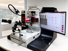
- Active alignment system with integrated heater and temperature sensor
- Laboratory/cleanroom space (900 m²)
Components
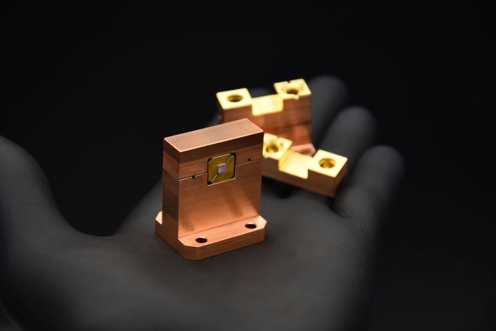
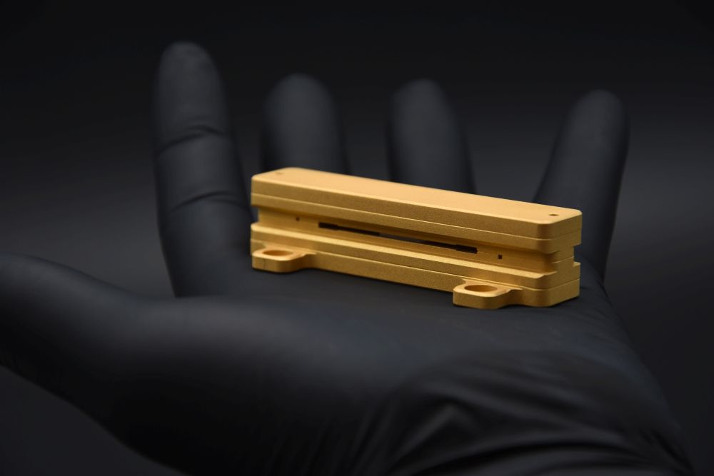
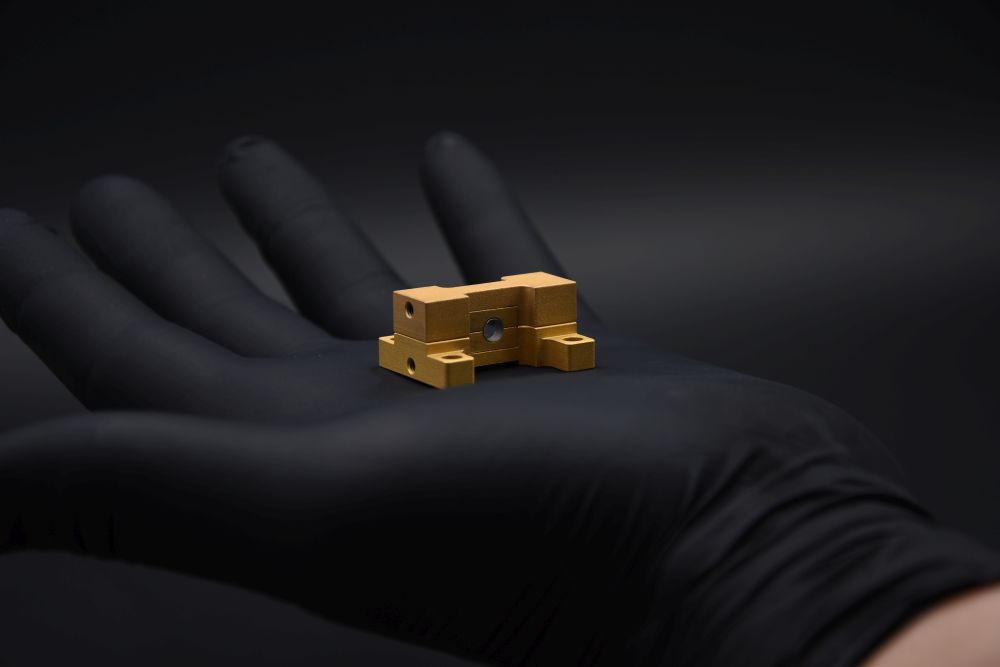
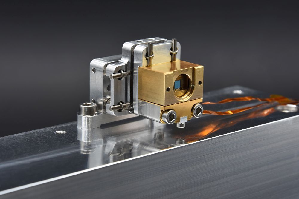
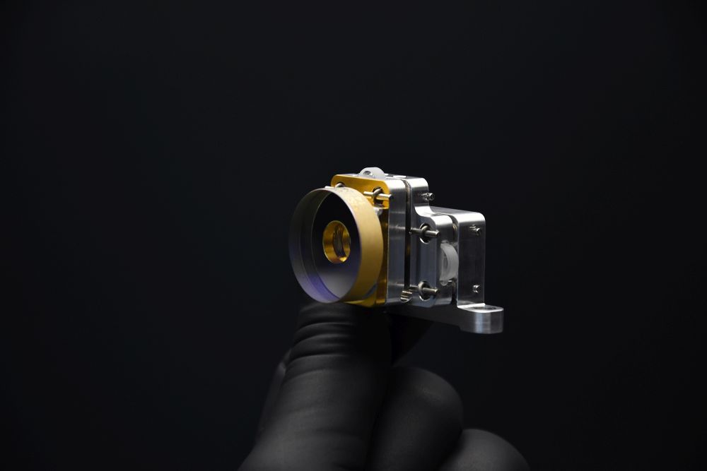
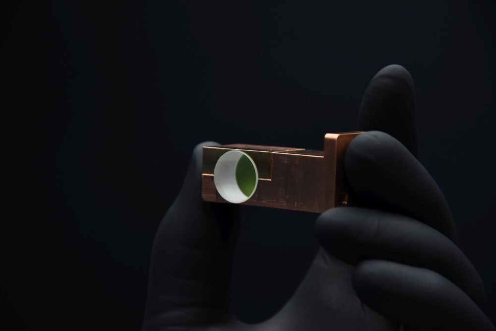
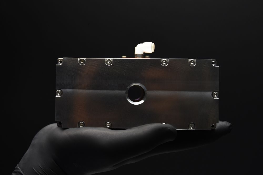
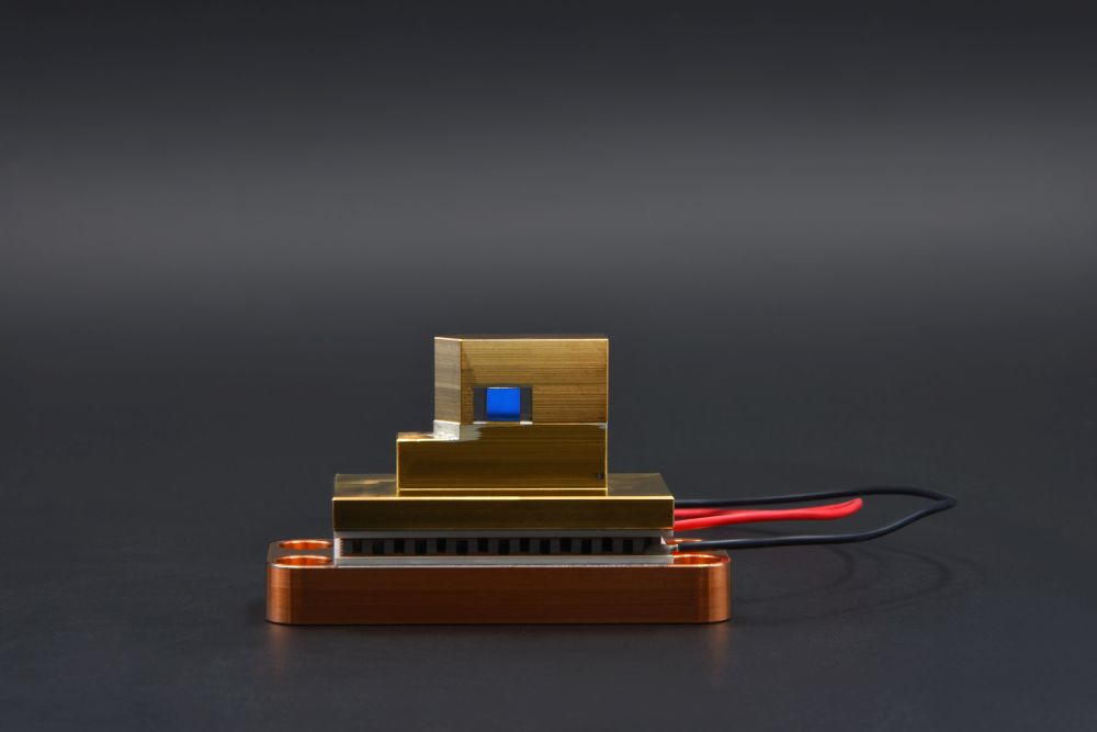
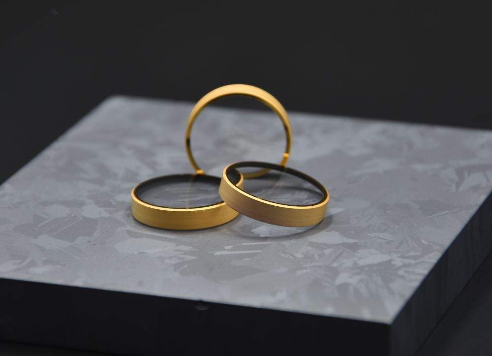
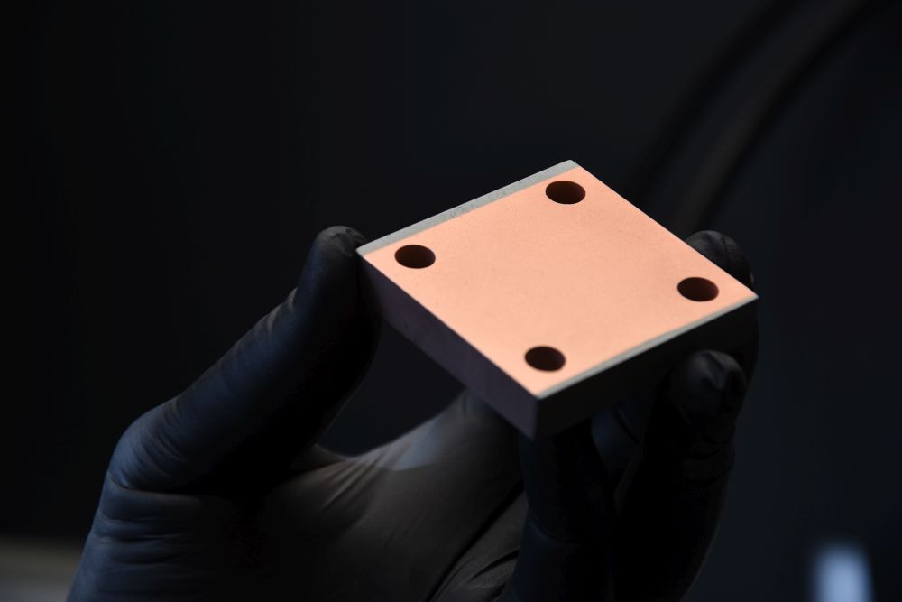
Inside the production
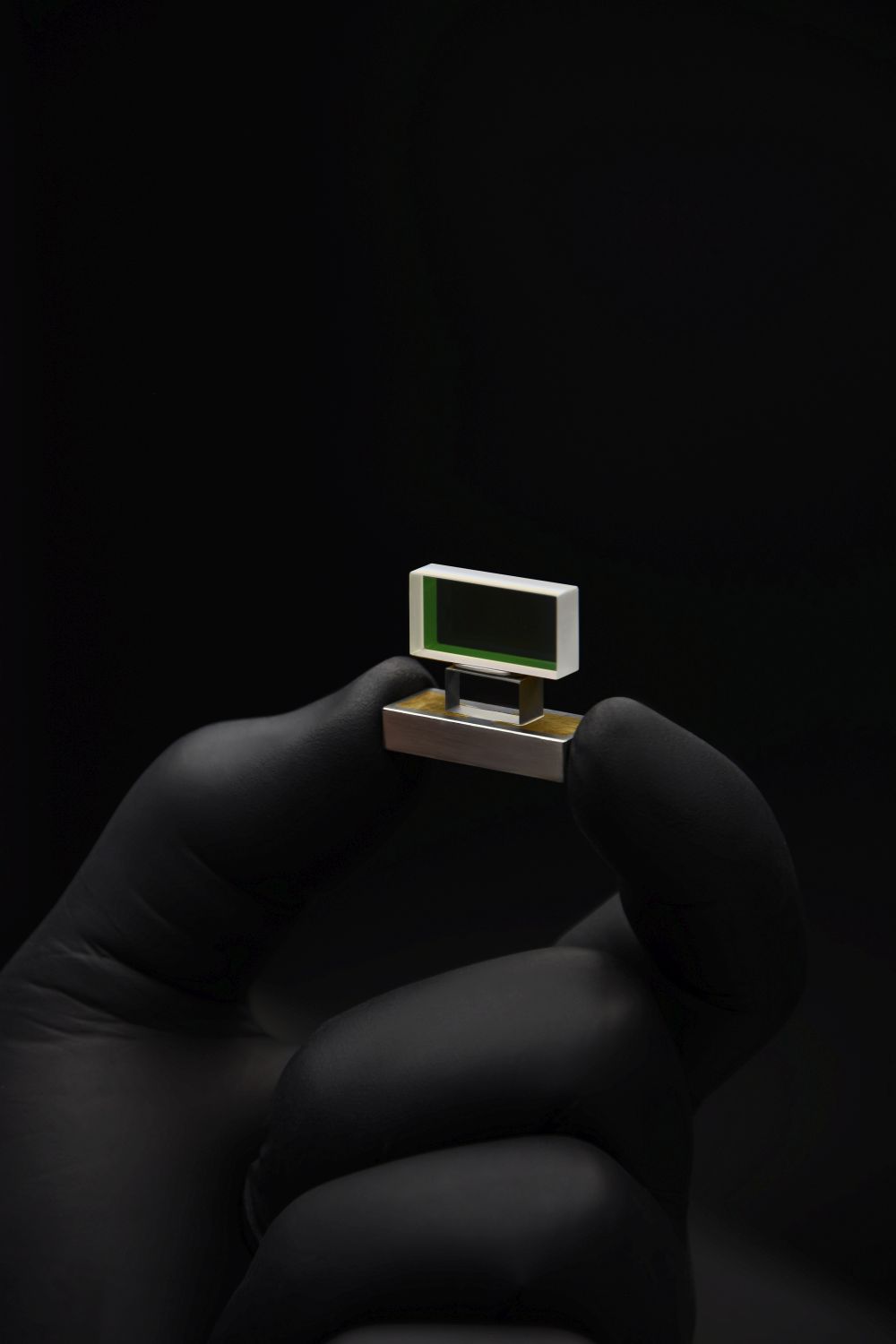
Industries
Processes & technical limits
| Processes | Tolerance | Max. part | Weight | Lot size | Materials |
|---|---|---|---|---|---|
| Flux-free vacuum soldering for optical, metallic & ceramic componentsJoining | – | – | – | Prototypes to series production | Glass, Metal, Ceramics |
| PVD deposition of solder layers (layer thicknesses 10–500 µm)Surface | – | – | – | – | Metals, Solders (metal) |
| Solderable metallization (magnetron sputtering)Surface | – | – | – | – | Glass, Metal, Ceramics |
| Sputter coatings on glass, metal, ceramicsSurface | – | – | – | – | Glass, Metal, Ceramics |
| Active alignment/soldering (Active Alignment) in a molten solder bath with integrated heaterAssembly | Sub-micron precision in alignment and bonding | – | – | – | Optical components |
| Laser crystal packaging (e.g. LCP-C Cube, Slab, Rod Geometry)Assembly | – | – | – | – | Laser crystals, Metal |
| Hermetic sealing technologies / hermetic jointsJoining | – | – | – | – | Optical components, Metal |
| Mechanical design and thermal simulationEngineering | – | – | – | – | – |
| Module development and assemblyAssembly | – | – | – | – | – |
| Environmental testing (temperature, humidity, shock)Testing | – | – | – | – | – |
| Electroplating processes (in cooperation with external partners)Surface | – | – | – | – | Metal |
4 Anlagen & Maschinen
| Machine | Manufacturer / model | Quantity | Working area | Year built | Site |
|---|---|---|---|---|---|
| PVD/sputter system for solder layer deposition and metallization | – | – | – | – | Herzogenrath |
| Vacuum soldering system | – | – | – | – | Herzogenrath |
| Active alignment system with integrated heater and temperature sensor | – | – | – | – | Herzogenrath |
| Laboratory/cleanroom space (900 m² production and office space) | – | – | 900 m² | – | Ericsson-Allee 1, 52134 Herzogenrath, Germany |
Additional services
Quality
PHOTONICPARTS performs environmental tests (temperature, humidity, shock) and builds processes with an integrated heater and temperature sensor for repeatable alignment; solder joints are hermetic, long-term stable and compatible with vacuum and space applications.
| Evidence | Herzogenrath |
|---|---|
| Environmental tests (temperature, humidity, shock) | |
| ISO 9001 |
History
- 2023-08
Founding of PHOTONICPARTS as a brand of XCCES GmbH by Dr. Jan Dolkemeyer and Phillip Dittmann in Herzogenrath
- 2023-08
Exhibition at CIOE 2023 (China International Optoelectronic Exposition)
- 2023-10
Alliance partner of LASER.region.AACHEN
- 2026-08
Expansion of in-house capacities for high-power laser diode packaging; 15 employees, distributors in China and Japan