Manufactures signal-enhancing plasmonic nanostructures for bioimaging and diagnostic applications.

Xfold Imaging Oy
Espoo, FinlandNew on Amplifa
About Xfold Imaging
Xfold Imaging Oy is a Finnish technology company founded in 2018 in alliance with Aalto University and the University of Helsinki. The company produces surface-signal-enhancing nanostructures for research and diagnostic applications, in particular for amplifying weak optical signals such as fluorescence, EUV and UCNP. Manufacturing is carried out by roll-to-roll nanoimprint lithography on substrates made of PET, polycarbonate and COC (thicknesses 125 and 250 µm, reflective and transparent) as well as on silicon and glass, cut to various sizes. Xfold chips are used in bioimaging (R&D laboratories), diagnostics (cancer, infectious diseases) and other optical systems and can be adapted to different imaging platforms such as microscopy slides, microfluidic devices and test cartridges. The product portfolio includes the Xfold Glass Slide, plasmonic rolls and sheets, and an E. coli detection kit. The company is based in the Micronova building in Espoo, which hosts the largest cleanroom environment in Northern Europe.
- Site
- Espoo, Finland
- Processes
- Roll-to-roll (R2R) nanoimprint lithography (plasmonic nanostructures), Production of Xfold plasmonic rolls / sheets (signal enhancer substrates), thickness 125 and 250 µm, Signal-enhancing nanostructures as substrates/slides, Adaptation to imaging platforms (microscopy slides, microfluidics, test cartridges), Roll-to-roll nanoimprint technology, E. coli detection kit
- Materials
- PET, PC (Polycarbonate), COC (Cycloolefin copolymer), Silicon, Glass, Polycarbonate, Polyethylene terephthalate, Cycloolefin copolymer
- Founded
- 2018
- Industries
- Bioimaging/Research laboratory, Diagnostics (cancer, infectious diseases), Photonics, Optical systems
- 01
Substrate production or substrate selection (PET, PC, COC, silicon, glass)
- 02
Roll-to-roll nanoimprint lithography of plasmonic nanostructures
- 03
Cutting to customer-specific sizes
- 04
Adaptation to imaging platforms (slides, microfluidics, test cartridges)
- 05
Use in bioimaging and diagnostics
Substrates & Processes
Polyethylene terephthalate
Flexible substrate for plasmonic rolls and sheets in reflective and transparent versions.
Polycarbonate
Robust polymer substrate for signal-enhancing nanostructures.
Cycloolefin copolymer
Optically suitable polymer substrate for plasmonic films.
Silicon
Rigid substrate for chip-based imaging and sensor applications.
Glass
Substrate for microscopy slides, e.g. the Xfold Glass Slide.
Locations
Micronova, Espoo
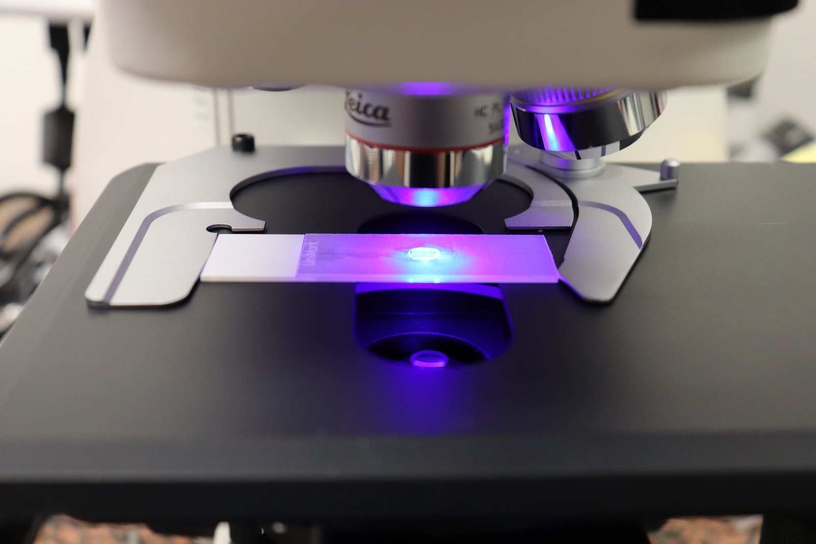
FIOffice and laboratory in the Micronova building with cleanroom environment
- Materials
- PET, PC, COC, silicon, glass
- Roll-to-roll nanoimprint lithography
- Cleanroom (Micronova)
Products & Components

Inside the production


Industries
Processes & technical limits
| Processes | Tolerance | Max. part | Weight | Lot size | Materials |
|---|---|---|---|---|---|
| Roll-to-roll (R2R) nanoimprint lithography (plasmonic nanostructures)Surface | – | – | – | – | PET, PC, COC, silicon, glass, polycarbonate |
| Production of Xfold plasmonic rolls / sheets (signal enhancer substrates), thickness 125 and 250 µmSurface | – | 125 um; 250 um (thickness) | – | – | PET, PC, COC |
Additional services
History
- 2018
Founding of Xfold Imaging Oy in alliance with Aalto University and the University of Helsinki.
- 2019
Introduction of the Xfold Glass Slide.
- 2023
Winner of the Photonics 21 Innovation Award at the Photonics 21 annual meeting on 26 April in Brussels.