Ist das Ihr Unternehmen? Profil übernehmen

Optische Systeme, Mikrooptik, Laser und optoelektronische Module für Halbleiter, Medizintechnik, Messtechnik und Smart Mobility
JENOPTIK AG
Jena · Berlin · Dresden · Triptis · Augsburg · Monheim am Rhein · Villingen-Schwenningen · Wedel · Wetzlar · AlgierNeu auf Amplifa
Über Jenoptik
JENOPTIK AG ist ein börsennotierter Technologiekonzern mit Sitz in Jena, der im Markt Photonik tätig ist. Das Unternehmen entwickelt und fertigt optische Systeme und Mikrooptik, optical Thin-Film-Elemente, diffraktive optische Elemente sowie Hochleistungslaser – von der epitaktischen Waferherstellung über die Fertigung optischer Komponenten bis zur Reinraum-Montage kompletter Systeme. Verfahren umfassen Präzisionsoptik aus optischen Gläsern, Kristallen und Kunststoffen, Beschichtung und Filterfertigung von DUV bis FIR, Spritzguss von Kunststoffoptiken, Lasermaterialbearbeitung, Werkzeugbau sowie optomechatronische Baugruppenmontage. Zu den Kunden zählen OEMs aus Halbleiter-Equipment, Medizintechnik und Life Science, Automotive, Maschinenbau, Messtechnik, Luft- und Raumfahrt sowie Sicherheits- und Verteidigungstechnik; im Bereich Verkehrsüberwachung bietet die Gruppe zudem Messsysteme, Kalibrier- und Serviceleistungen. Als OEM-Entwicklungs- und Produktionspartner übernimmt Jenoptik die gesamte Wertschöpfungskette inklusive Supply-Chain-Management für Kunden. In Deutschland fertigt die Gruppe an Standorten in Jena, Berlin, Dresden, Triptis, Augsburg, Monheim am Rhein, Villingen-Schwenningen, Wedel und Wetzlar; weltweite Standorte bestehen in Europa, Amerika, Afrika und Asien-Pazifik.
- Standort
- Jena
- Verfahren
- Laser systems for cutting of plastics, metals and sensitive materials, Laser welding of plastics, metals and sensitive materials, Laser perforating of plastics, metals and sensitive materials, Laser marking, Laser welding (of metal and plastic), Laser cutting, Laser drilling, Laser structuring and removal
- Werkstoffe
- Optical glass SiO2, Silicon, Germanium, Zinc selenide, Sapphire, Magnesium fluoride, Calcium fluoride, GaAs compound semiconductors (Al, In, Ga)(As, P)
- Zertifikate
- ISO 9001:2015, ISO 14001:2015, ISO 50001:2018, ISO 13485:2016, ISO 9001:2015 (JENOPTIK Optical Systems LLC, Huntsville, USA), ISO 9001:2015 (JENOPTIK Optical Systems LLC, Jupiter, USA), ISO 9001:2015 (JENOPTIK Shanghai), ISO 37301 (Compliance-Management), AEO-F (Zugelassener Wirtschaftsbeteiligter, JENOPTIK Robot GmbH), TISAX (Informationssicherheit Automotive), ISO 9001, ISO 14001, ISO 13485, ISO 50001, TISAX, ISO 45001
- Gegründet
- 1990 (JENO
- Mitarbeiter
- 4.500 (Weltweit,
- Branchen
- Halbleiter- und Halbleiter-Equipment, Medizintechnik und Life Science, Automotive und Zulieferer, Maschinenbau und Anlagenbau, Industrielle Messtechnik, Verkehrssicherheit und Smart Mobility
- 01
Engineering und OEM-Co-Development
- 02
Epitaxiales Waferwachstum und Halbleiterfertigung
- 03
Optik- und Mikrooptikfertigung
- 04
Optische Beschichtung und Filterfertigung
- 05
Spritzguss von Kunststoffoptiken und Werkzeugbau
- 06
Lasermaterialbearbeitung
- 07
Montage und Integration (Reinraum)
- 08
Prüfung, Test- und Kalibriertechnik
- 09
Supply-Chain-Management und Kundenservice
Werkstoffe und Verfahren
Optisches Glas (SiO2)
Grundwerkstoff für präzise optische Komponenten und Systeme.
Silizium
Optisches Material für Infrarot- und Halbleiteranwendungen.
Germanium
Infrarotoptisches Material für thermische Anwendungen.
Zinkselenid
IR-Transparentes Material für Laser- und Thermaloptik.
Magnesiumfluorid
Kristallwerkstoff für optische Komponenten im UV- bis IR-Bereich.
Calciumfluorid
Kristallwerkstoff für hochauflösende UV-Optik.
GaAs-Verbundhalbleiter (Al, In, Ga)(As, P)
Substratmaterial für Laserbars und Single Emitters.
Nd:YVO4
Laserkristall für frequenzverdoppelte Thin-Disk-Laser.
Optische Kunststoffe (Polymere)
Spritzgegossene Polymeroptiken für miniaturisierte Systeme.
Diamond-Like Carbon (DLC)
Verschleißfeste Beschichtung für optische Oberflächen.
Bauteile
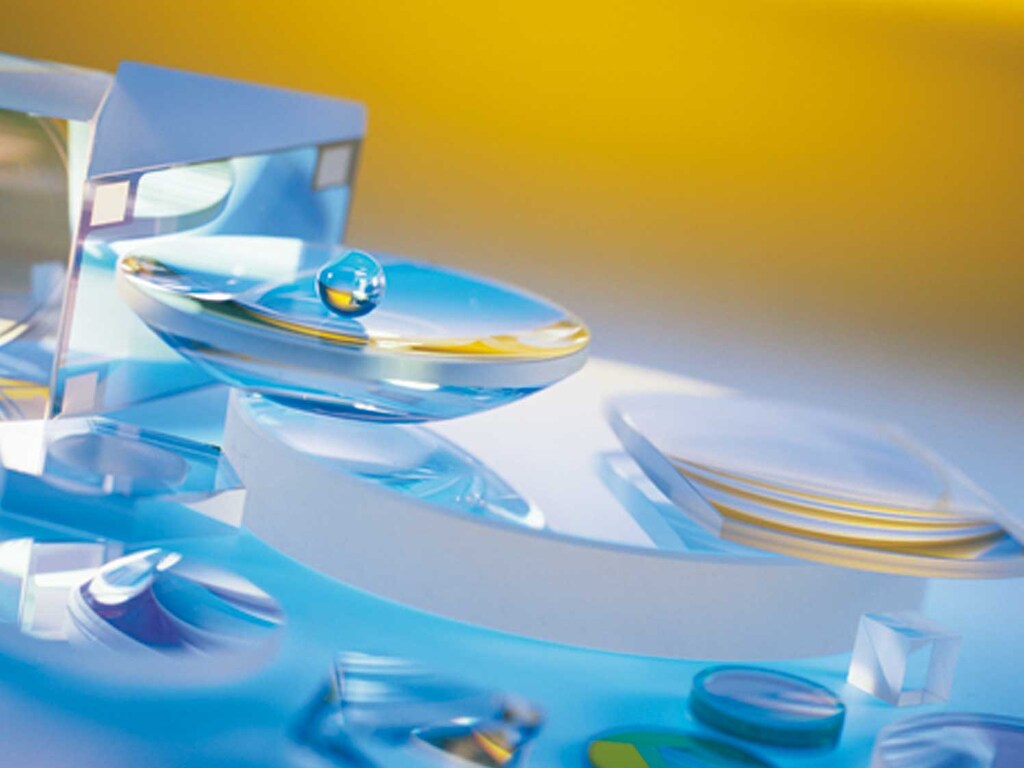
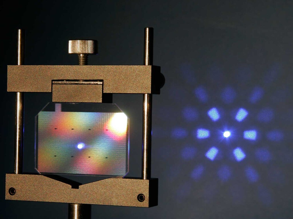
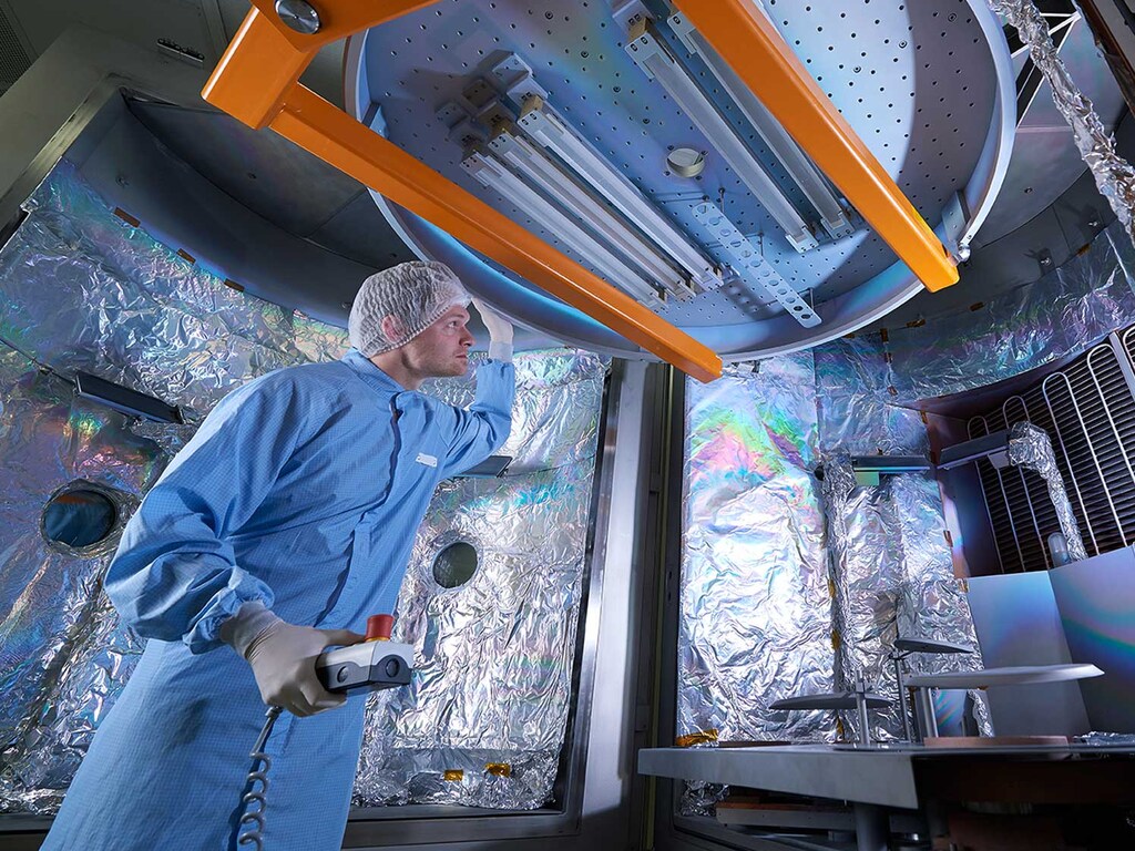
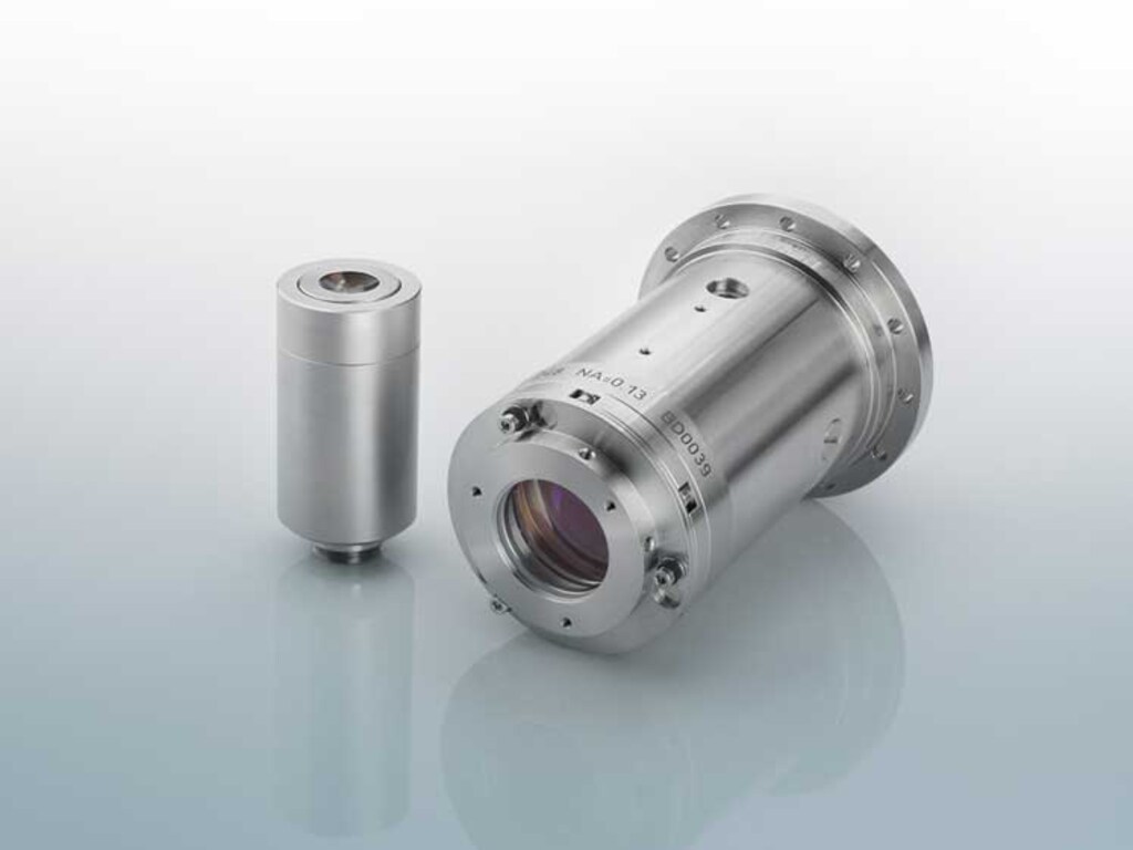
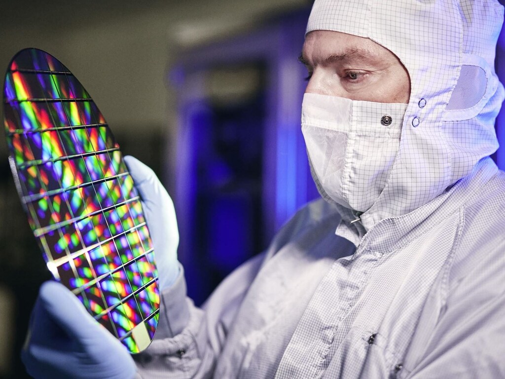
Einblicke in die Fertigung
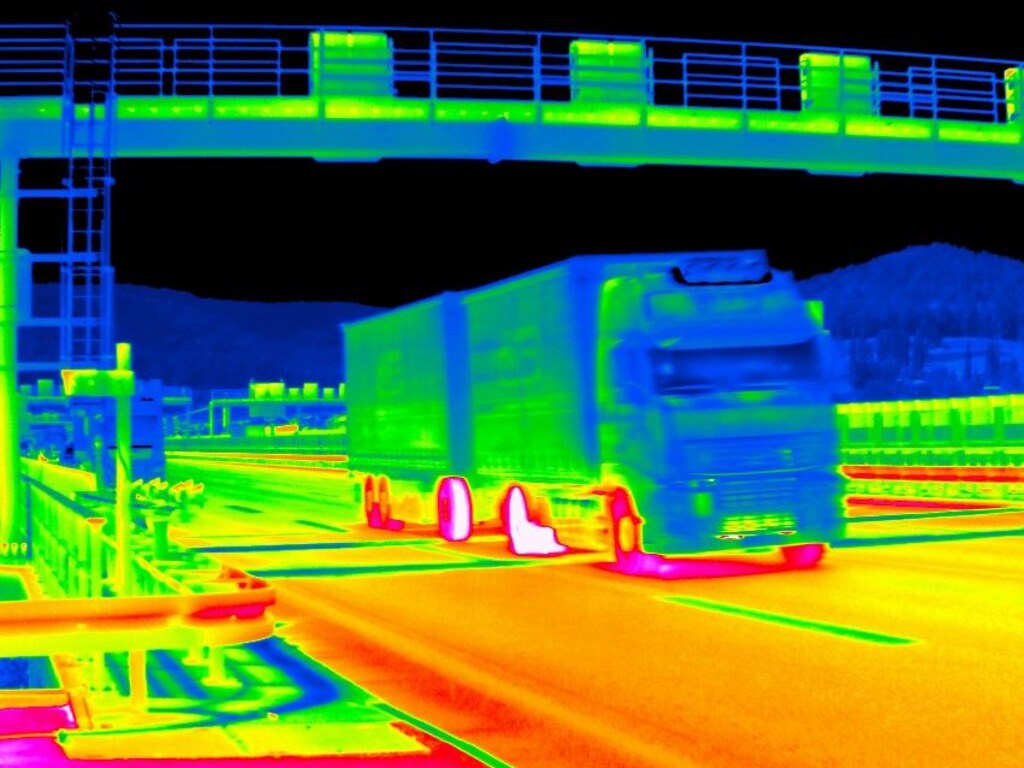
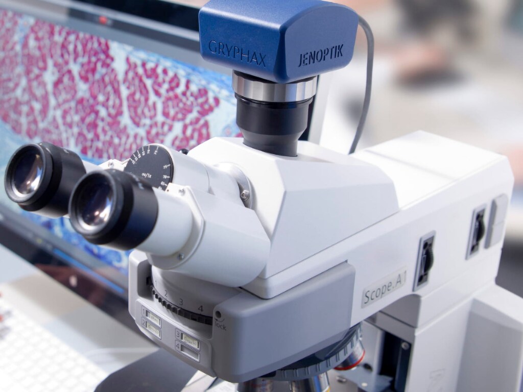
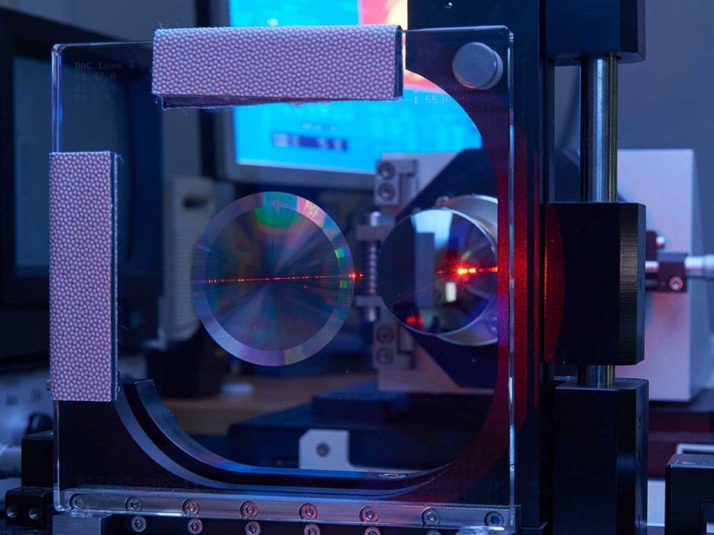
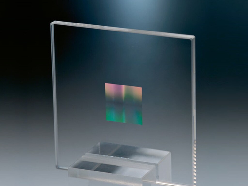
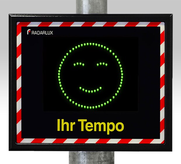
Branchen
Verfahren & technische Grenzen
| Verfahren | Toleranz | Max. Bauteil | Gewicht | Losgröße | Werkstoffe |
|---|---|---|---|---|---|
| Laser systems for cutting of plastics, metals and sensitive materialsLaser material processing | – | – | – | – | plastics, metals, sensitive materials |
| Laser welding of plastics, metals and sensitive materialsLaser material processing | – | – | – | – | plastics, metals, sensitive materials |
| Laser perforating of plastics, metals and sensitive materialsLaser material processing | – | – | – | – | plastics, metals, sensitive materials |
| Laser markingLaser material processing | – | – | – | – | metals, polymers, substrates, ceramics |
| Laser welding (of metal and plastic)Laser material processing | – | – | – | – | metal, plastic |
| Laser cuttingLaser material processing | – | – | – | – | plastic, metal |
| Laser drillingLaser material processing | – | – | – | – | metals, polymers, substrates, ceramics |
| Laser structuring and removalLaser material processing | – | – | – | – | metals, polymers, substrates, ceramics |
| Selective laser solderingFügen | – | – | – | – | – |
| Laser engravingLaser material processing | – | – | – | – | – |
| Laser cleaningLaser material processing | – | – | – | – | – |
| Laser ablationLaser material processing | – | – | – | – | – |
| Laser scoring for airbag applications (contact-free processing of plastic components)Laser material processing | – | – | – | – | plastic |
| Laser tire carvingLaser material processing | – | – | – | – | rubber/tires |
| Epitaxial wafer growth (compound semiconductors (Al, In, Ga)(As, P))Semiconductor manufacturing | – | – | – | – | GaAs, AlGaAs, InGaAsP |
| Semiconductor fab for processing GaAs-based optoelectronic devices; manufacture of compoundSemiconductor manufacturing | – | – | – | – | GaAs |
| High-power diode laser assembly and packaging (760-1060 nm, output power levels up to 300 W in cwLaser manufacturing | – | – | – | – | GaAs, AlGaAs |
| Manufacture of diode-pumped thin disk lasers (frequency-doubled 532 nm thin disk Nd:YVO4 lasers)Laser manufacturing | – | – | – | – | Nd:YVO4 |
| Manufacture of fiber lasers (JenLas fiber ns 25-105 for industrial marking and micromachining)Laser manufacturing | – | – | – | – | – |
| Manufacturing of optical coatings and filters (narrowband and bandpass filters, edge filters,Beschichtung | – | – | – | – | optical glass, polymer optics |
| Diamond-like carbon (DLC) coating of opticsBeschichtung | – | – | – | – | optical glass |
| Injection molding of sophisticated polymer optical componentsSpritzguss | – | – | – | – | plastic/polymers |
| Development and production of high-precision injection molding (endoscopy miniaturization)Spritzguss | accuracy of 1 µm for chip-prism assembly | – | – | – | plastic/polymers |
| Tool and mold design and constructionWerkzeugbau | – | – | – | – | – |
| Surface technologyOberflächenbearbeitung | – | – | – | – | – |
| Opto-mechanical and optoelectronic assembly; cleanroom assemblyMontage | – | – | – | – | – |
| Manufacture of optical systems, microoptics and high-end objective lenses (DUV to FIR); opticalOptikfertigung | – | – | – | – | optical glass (SiO2, Si, Ge, ZnSe, Sapphire, MgF2, CaF2), polymers |
| State-of-the-art alignment and bonding technologies (chip-prism assembly for endoscopy,Montage | accuracy of 1 µm for the entire chip-prism assembly | – | – | – | – |
| Assembly of laser system components (from laser components to automated laser machines, robot-basedMontage | – | – | – | – | – |
| Development, manufacturing and sales of optical test & measurement instruments and equipment forMess- und Prüftechnik | – | – | – | – | – |
| Development, production, sales and service of industrial metrology productsMess- und Prüftechnik | – | – | – | – | – |
| Manufacture of optomechatronic assemblies for medical applicationsMontage | – | – | – | – | – |
| Manufacture of hardware and software systems and components of optics, laser technology, digitalOptikfertigung | – | – | – | – | – |
| Manufacture of exhaust air purification systems (removal of pollutants and aerosols from productionSystemfertigung | – | – | – | – | – |
| Assembly and alignment of LiDAR systems (TRIOPTICS application-oriented solution for alignment andMontage | – | – | – | – | – |
Zusatzleistungen
Referenzkunden
Qualität und Zertifizierungen
Die Qualitätsmanagementsysteme der Geschäftsbereiche werden jährlich auditiert; 100 % der Fertigungsstandorte sind nach ISO 9001 bzw. ISO 13485 zertifiziert. Prüf- und Kalibriertechnik, u. a. TRIOPTICS-Messtechnik und DAkkS-DKD-Akkreditierung der Industriellen Messtechnik, überwachen Produkte und Prozesse.
| Nachweis | Jena | Berlin | Dresden | Triptis | Villingen-Schwenningen | Wedel | Wetzlar |
|---|---|---|---|---|---|---|---|
| ISO 9001 | |||||||
| ISO 14001 | |||||||
| ISO 13485 | |||||||
| ISO 50001 | |||||||
| TISAX | |||||||
| ISO 45001 |
Historie
- 1846
Carl Zeiss eröffnet seine optische Werkstatt in Jena – Ursprung des Unternehmens.
- 1948
Carl-Zeiss-Stiftung und neues Zeiss-Unternehmen in Baden-Württemberg; das Zeiss-Werk Jena geht in Volkseigentum über.
- 1990
Gründung der JENOPTIK Carl Zeiss Jena GmbH.
- 1991
Entstehung der JENOPTIK GmbH als staatliches Unternehmen.
- 1996
Die JENOPTIK AG entsteht.
- 1998
Börsengang der JENOPTIK AG an der Frankfurter Börse.
- 2020
RADARLUX Radar Systems GmbH wird zum 10.08.2020 in die JENOPTIK Robot GmbH integriert.