Ist das Ihr Unternehmen? Profil übernehmen
Customized VCSELs, VCSEL-Arrays, LEDs und Photodioden – mit Cleanroom, Assembly und Test in Ulm.

Vertical Photonics GmbH
UlmNeu auf Amplifa
Photonik-Engineering von Device Physics bis Packaging
Vertical Photonics ist ein Photonik-Engineering-Dienstleister mit Sitz im Science Park II in Ulm. Das Unternehmen entwickelt und fertigt customized VCSELs und VCSEL-Arrays, LEDs (Visible und NIR) sowie Hochgeschwindigkeits-Photodioden mit spektraler Abdeckung von UV bis IR. Das Leistungsspektrum umfasst den gesamten Stack: Device- und Maskendesign, Custom-Epitaxie-Strukturdesign, Rapid Prototyping, Small-Volume-Production, Cleanroom-Dienstleistungen (Metallkontakte, Etching, Passivation, Nassoxidation, Grinding/Polishing, Dicing), Chip-on-Board-Assembly mit Eutectic- und Epoxy-Die-Attach sowie Au-/Al-Wire- und Ribbon-Bonding und Flip-Chip, Packaging in TO-Cans, auf Keramik-Submounts und in Custom Housings sowie Wafer- und Die-Test mit L-I-V, spektralen und Beam-Profile-Messungen. Abnehmerbranchen sind Data Communications, Sensing & LiDAR, Medical & Life Sciences, industrielle Messtechnik, Consumer Electronics sowie Defense & Aerospace. Zielgruppe sind Forschungsgruppen, die einzelne kundenspezifische Bauelemente benötigen, ebenso wie OEMs mit Bedarf an wiederholbarer Versorgung mit verpackten Emittern. Die Fertigung erfolgt in Kleinserien mit Prozess-Lock, SPC, Reliability-Stress und voller Lot-Traceability.
- Standort
- Ulm
- Verfahren
- VCSEL-Fertigung (customized single- & multi-mode VCSELs, VCSEL-Arrays), LED-Herstellung (Visible & NIR LEDs), Photodioden-Fertigung (UV bis IR, High-Bandwidth), Consultancy & Advisory (Device & Package Architecture, Epi-Design), Rapid Prototyping (Short-loop fab & test, L-I-V, spectral, beam-profile), Small-Volume Production (Process lock, SPC, lot traceability), Eutectic & epoxy die attach, Au & Al wire bonding, ribbon bonding
- Werkstoffe
- Gold (Bonddraht), Aluminium (Bonddraht), Keramik (Submounts), Epoxy (die attach), Eutectic-Lötmaterial, VCSEL/LED/Photodiode-Halbleiter (III-V-Verbindungshalbleiter, implizit), Gold, Aluminium
- Zertifikate
- Lot traceability & SPC, Reliability stress testing, ISO 9001
- Branchen
- Data Communications, Sensing & LiDAR, Medical & Life Sciences, Industrial Metrology, Consumer Electronics, Defense & Aerospace
- 01
Consulting & Spezifikation
- 02
Device- und Epi-Design / Simulation
- 03
Short-Loop-Fabrikation (Cleanroom)
- 04
Chip-on-Board-Assembly (Die Attach, Bonding, Flip-Chip)
- 05
Packaging
- 06
Wafer- und Die-Test / Charakterisierung
- 07
Small-Volume-Production mit Qualifikation
Materialien und Verfahren
Gold
Bonddraht und Ribbon-Bonding für photonische Chipverbindungen.
Aluminium
Bonddraht-Material für Chip-on-Board-Assembly.
Eutectic-Lötmaterial
Die-Attach mit thermisch und elektrisch leitfähiger Verbindung.
Epoxy
Die-Attach-Material für Assembly-Prozesse.
Keramik
Submount-Material für Packaging.
III-V-Halbleiter (VCSEL/LED/Photodiode)
Basismaterial der gefertigten photonischen Bauelemente.
Standort
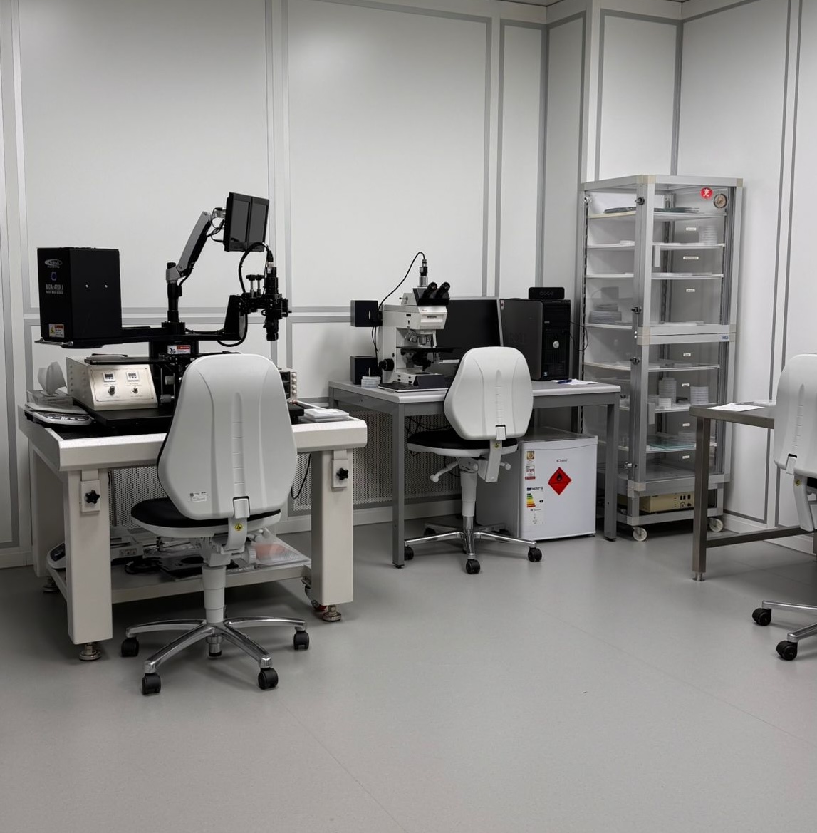
Ulm
DEHauptsitz mit Cleanroom, Assembly & Test
- Losgröße
- Prototyp bis Kleinserie
- Werkstoffe
- III-V-Halbleiter, Gold, Aluminium, Keramik, Epoxy, Eutectic-Lot
- Cleanroom
- Lithographie / Mask-Alignment
- Metal Evaporation System
- Wet Bench
- Dicing equipment
- Wire bonder / Die attach
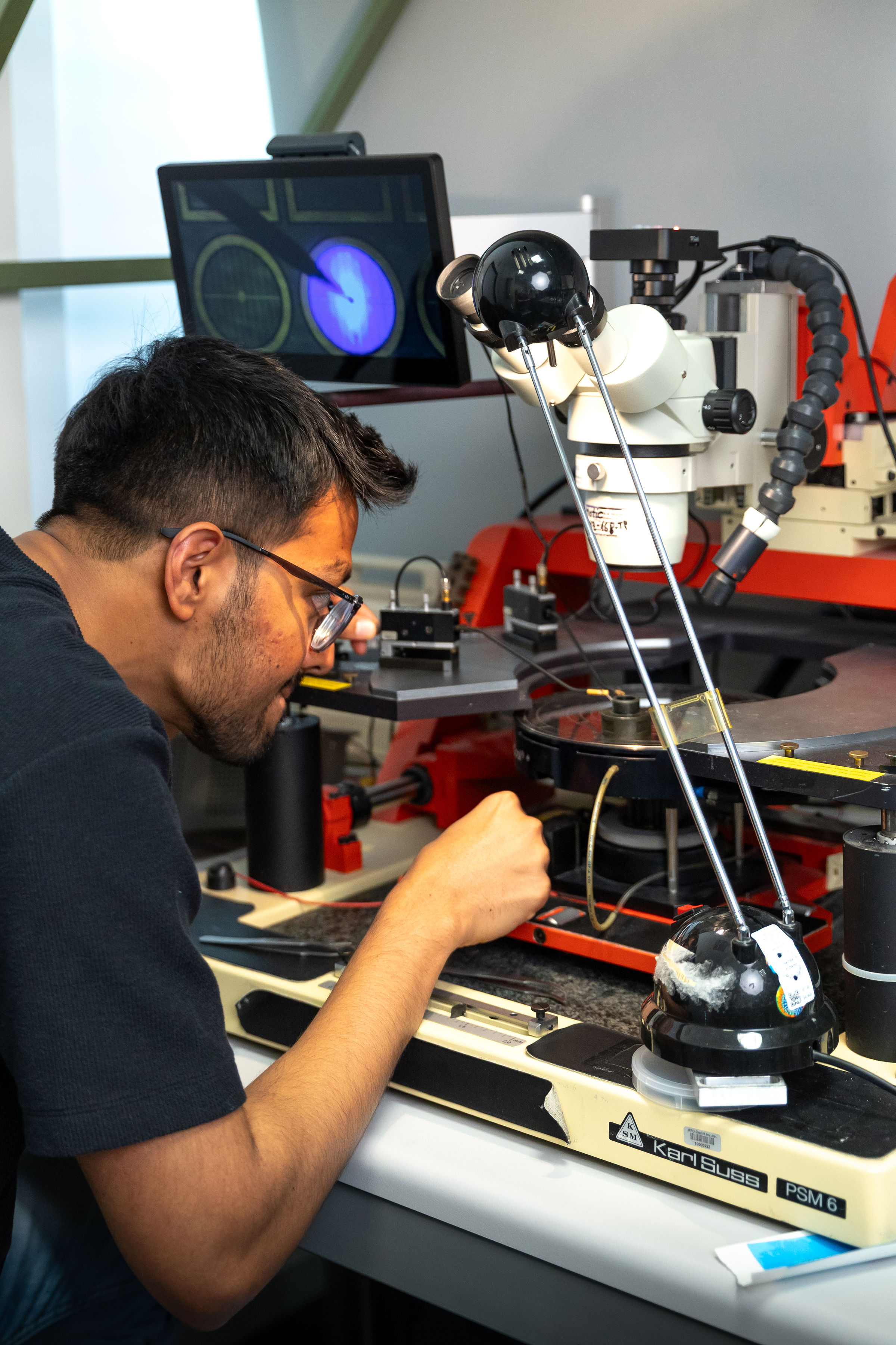
- Probe station
- Automated die tester & tape sorter
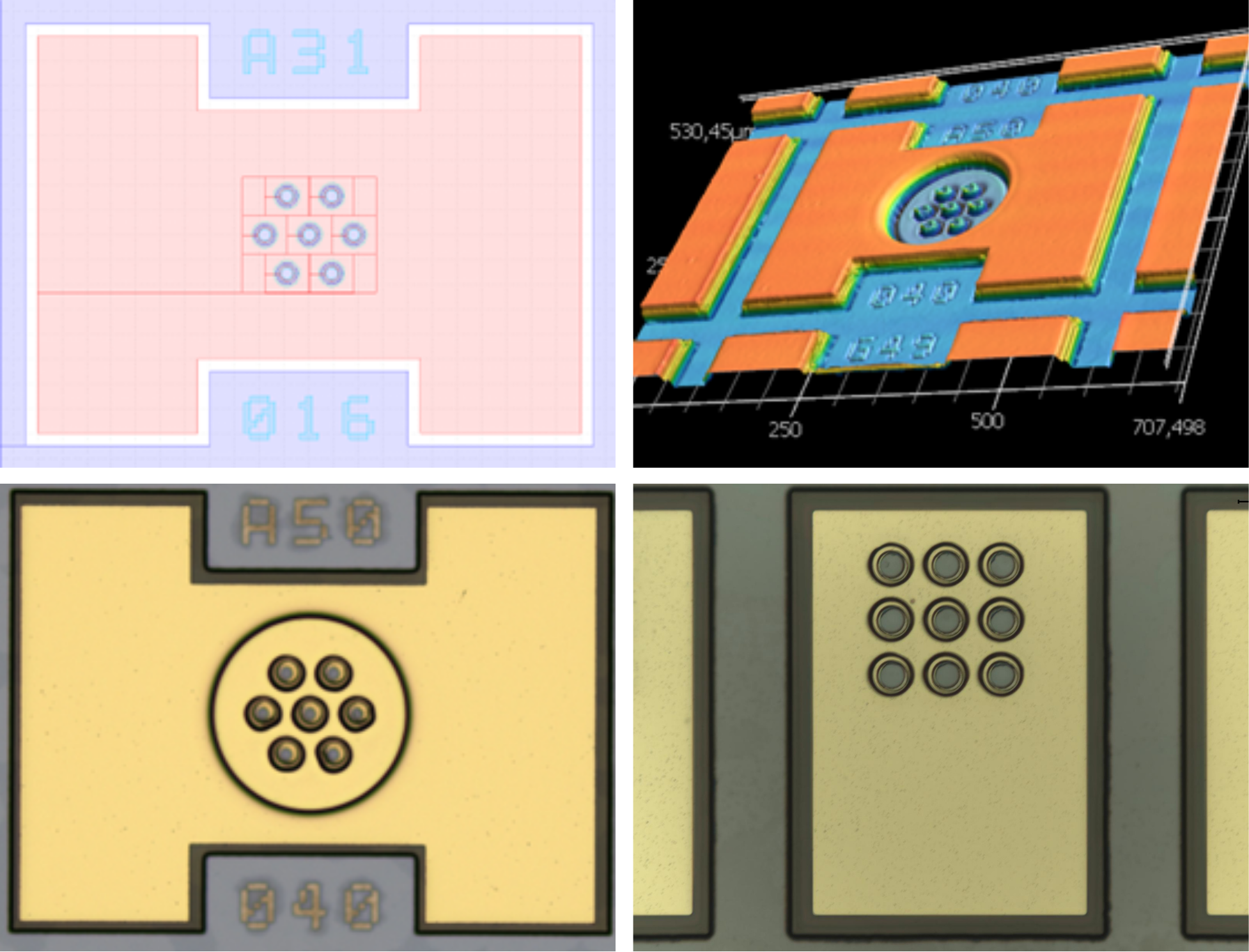
- 3D profile measurement system
Bauelemente
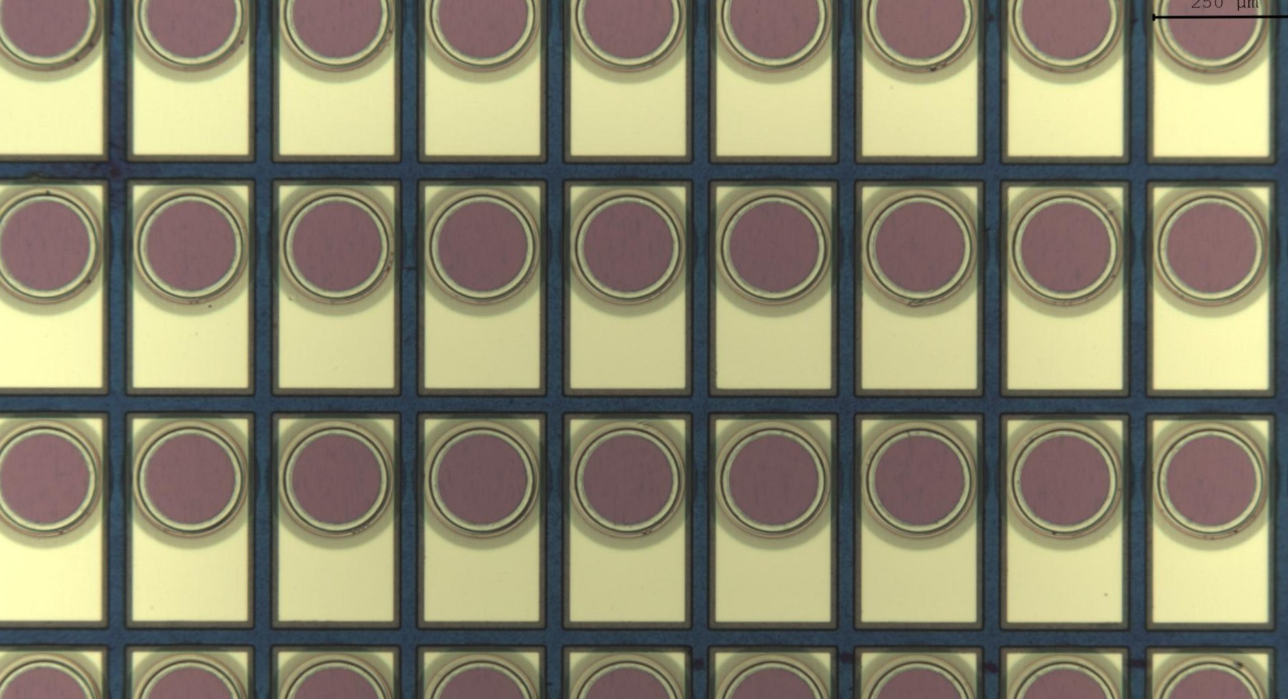
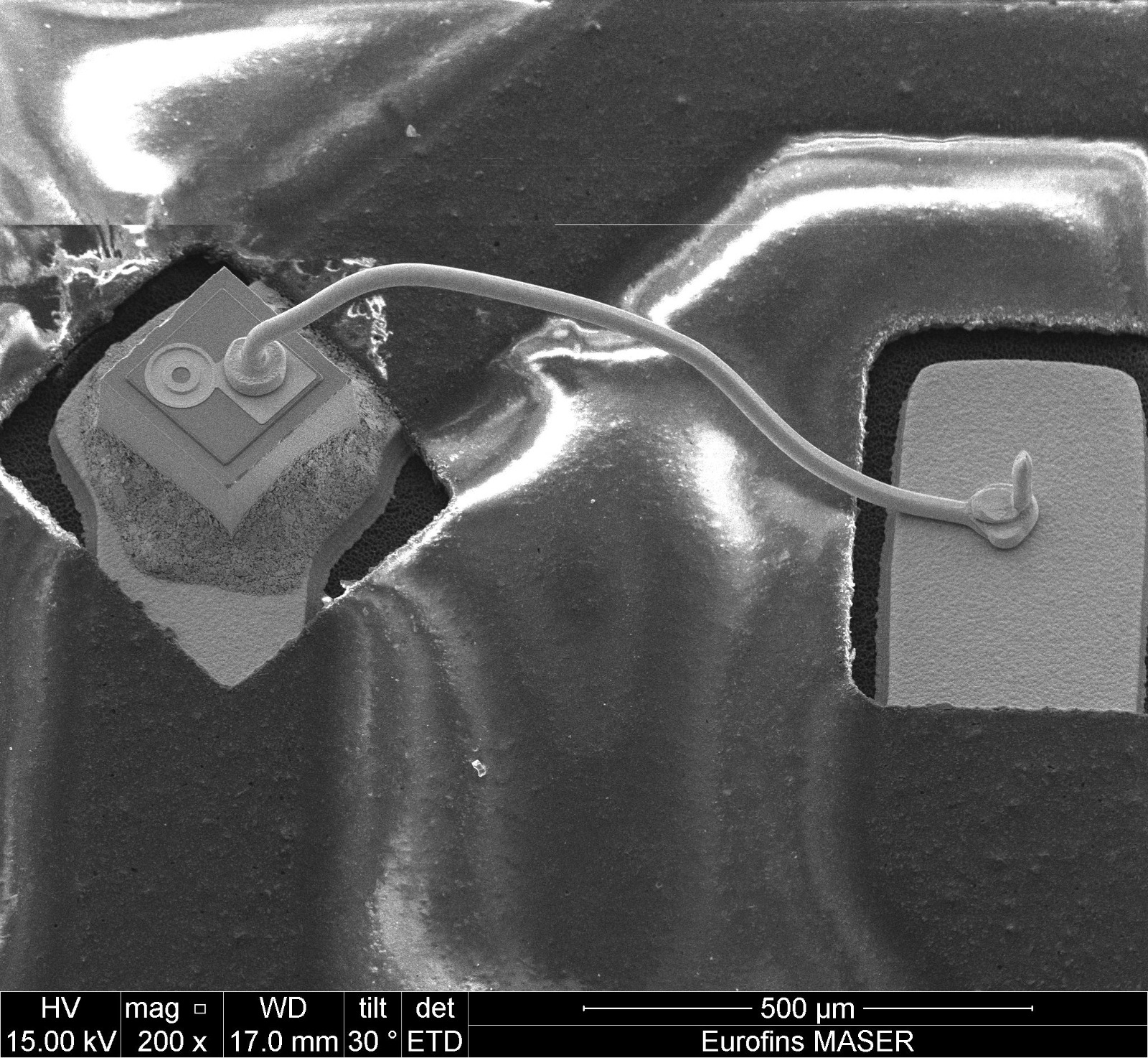
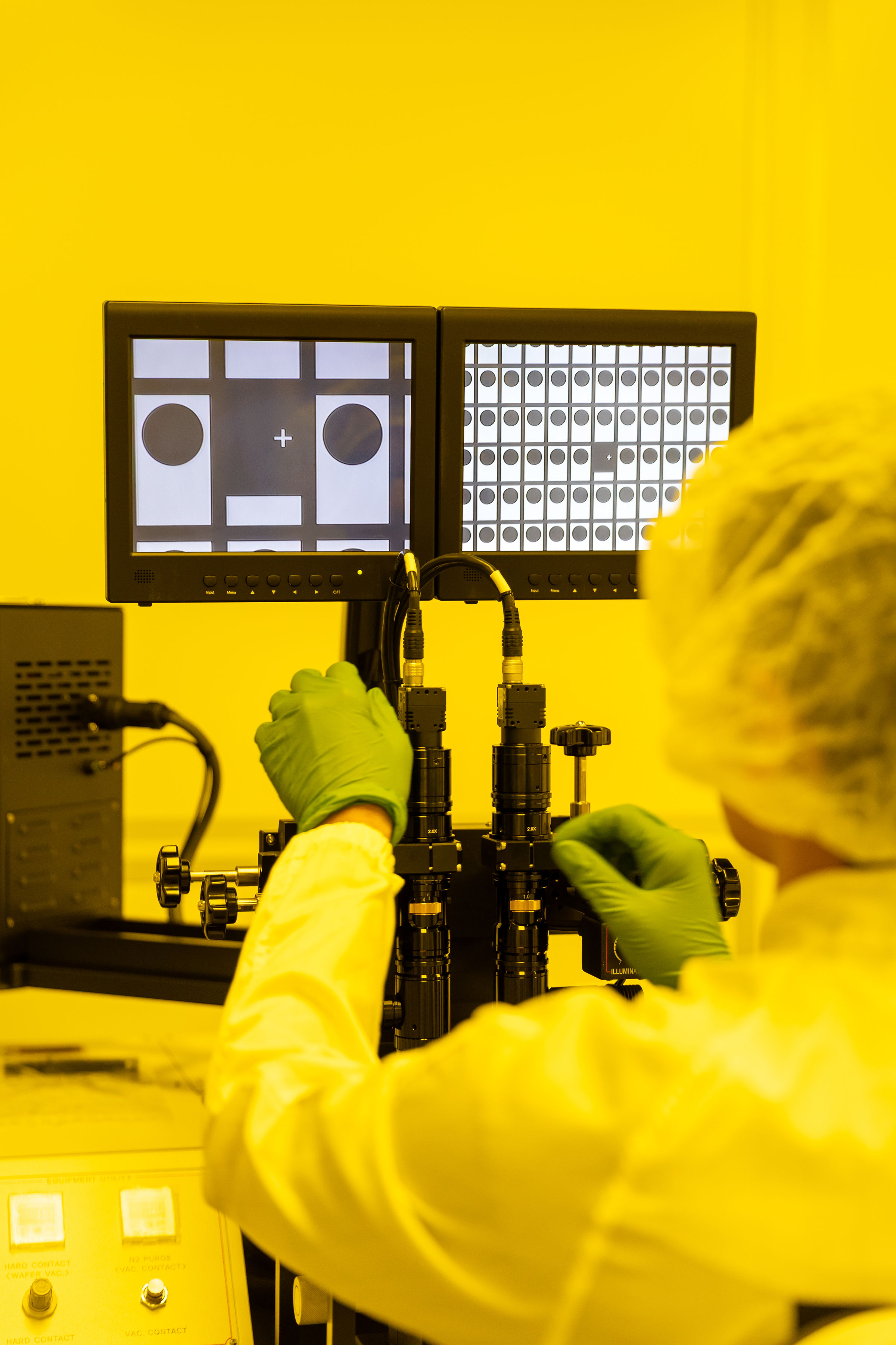
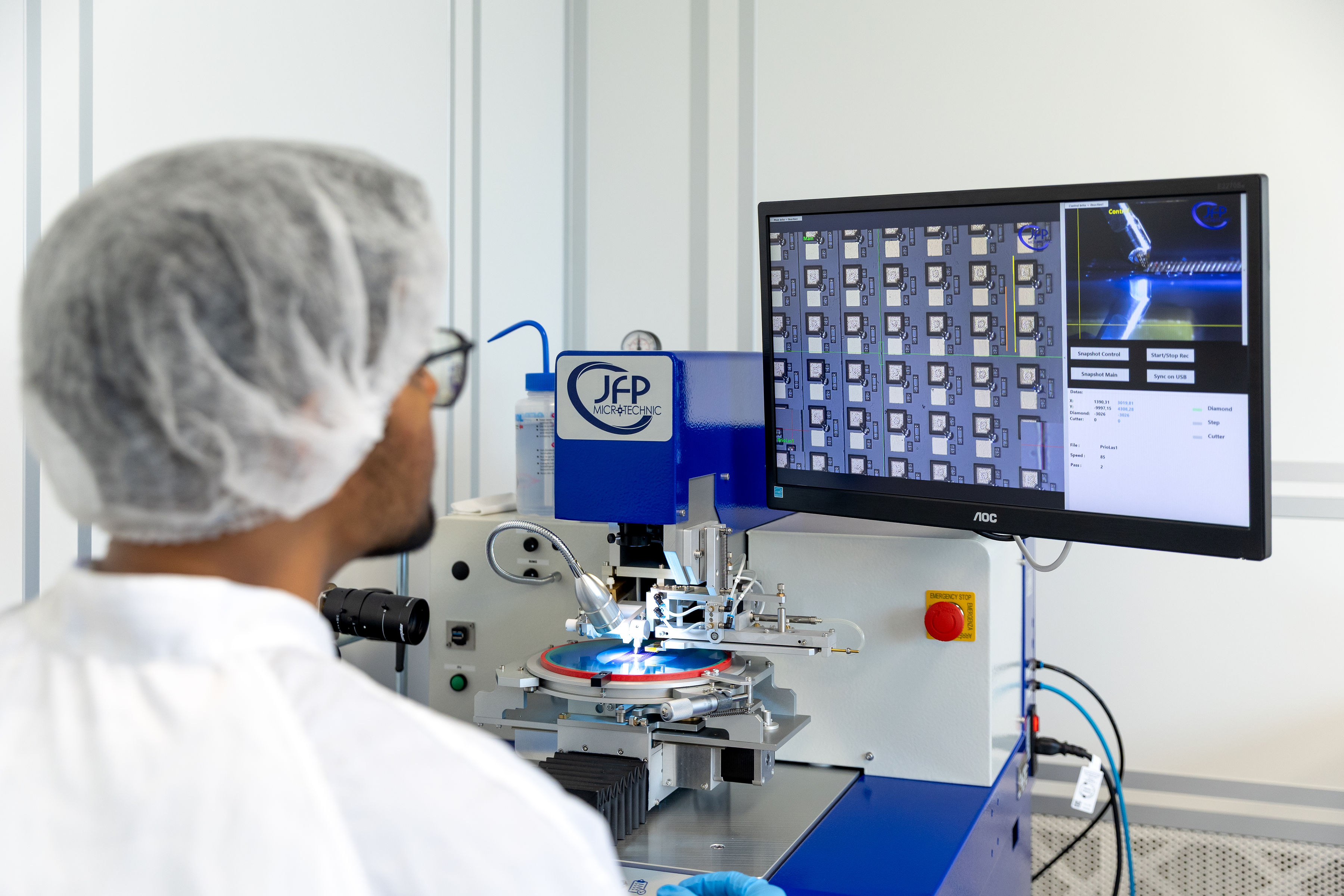
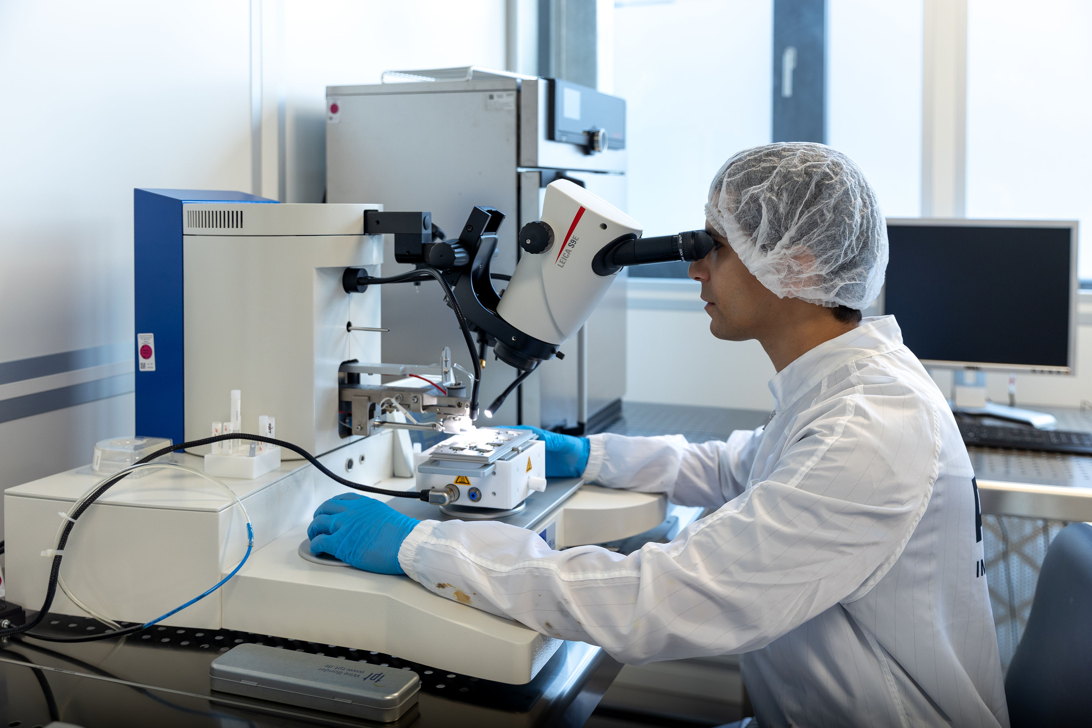
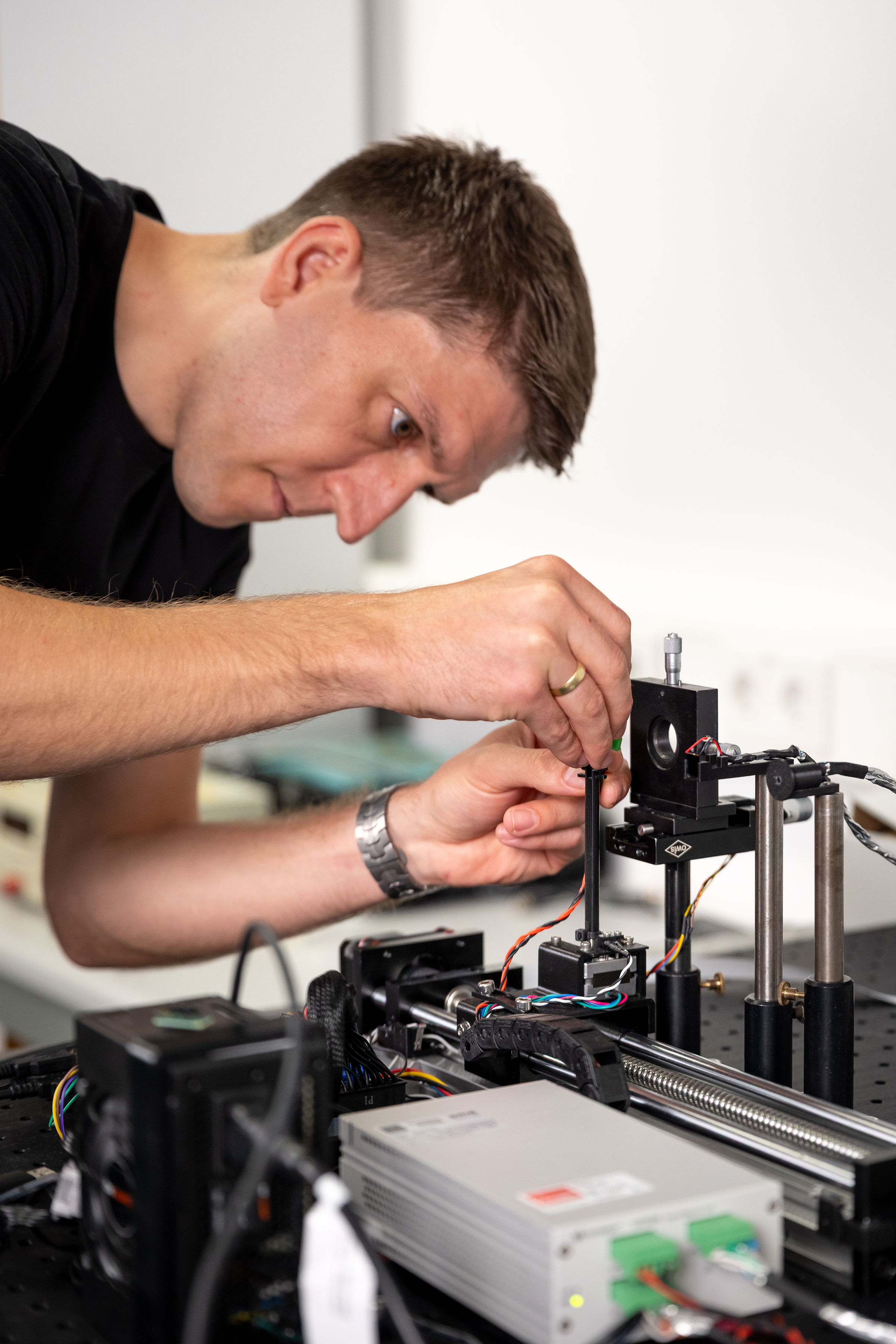
Einblicke in die Fertigung
Branchen
Verfahren & technische Grenzen
| Verfahren | Toleranz | Max. Bauteil | Gewicht | Losgröße | Werkstoffe |
|---|---|---|---|---|---|
| VCSEL-Fertigung (customized single- & multi-mode VCSELs, VCSEL-Arrays)Halbleiter/Photonics (Herstellung photonischer Komponenten) | – | – | – | Small-Volume Production | GaAs-basierte Halbleiter (implizit, VCSEL) |
| LED-Herstellung (Visible & NIR LEDs)Halbleiter/Photonics | – | – | – | – | Halbleiter |
| Photodioden-Fertigung (UV bis IR, High-Bandwidth)Halbleiter/Photonics | – | – | – | – | Halbleiter |
| Consultancy & Advisory (Device & Package Architecture, Epi-Design)Engineering | – | – | – | – | – |
| Rapid Prototyping (Short-loop fab & test, L-I-V, spectral, beam-profile)Engineering | – | – | – | – | – |
| Small-Volume Production (Process lock, SPC, lot traceability)Halbleiter/Photonics | – | – | – | – | – |
| Eutectic & epoxy die attachFügen | – | – | – | – | Halbleiter-Chips |
| Au & Al wire bonding, ribbon bondingFügen | – | – | – | – | Gold, Aluminium |
| Flip-chip assemblyFügen | – | – | – | – | Halbleiter-Chips |
| Hermetic & non-hermetic packaging (TO-cans, ceramic submounts, custom housings)Montage | – | – | – | small-series production | Keramik, Metall |
| Metal contacts / Metal evaporationOberfläche | – | – | – | – | Metalle |
| EtchingHalbleiterprozesstechnik | – | – | – | – | – |
| PassivationHalbleiterprozesstechnik | – | – | – | – | – |
| Wet thermal oxidationHalbleiterprozesstechnik | – | – | – | – | – |
| Grinding & polishingOberfläche | – | – | – | – | – |
| Dicing & wafer singulationHalbleiterprozesstechnik | – | – | – | – | – |
| Lithography — multi-layer mask alignmentHalbleiterprozesstechnik | – | – | – | – | – |
| Wet bench processingHalbleiterprozesstechnik | – | – | – | – | – |
| Custom epitaxial structure designEngineering | – | – | – | – | – |
| Device & mask design (custom LED & VCSEL layouts)Engineering | – | – | – | – | – |
| Wafer & die test (probe-station characterization, automated L-I-V, spectral, beam-profile)Prüfung | – | – | – | – | – |
| Electrical characterizationPrüfung | – | – | – | – | – |
| Optical characterizationPrüfung | – | – | – | – | – |
| Automated die testing & tape sortingPrüfung | – | – | – | – | – |
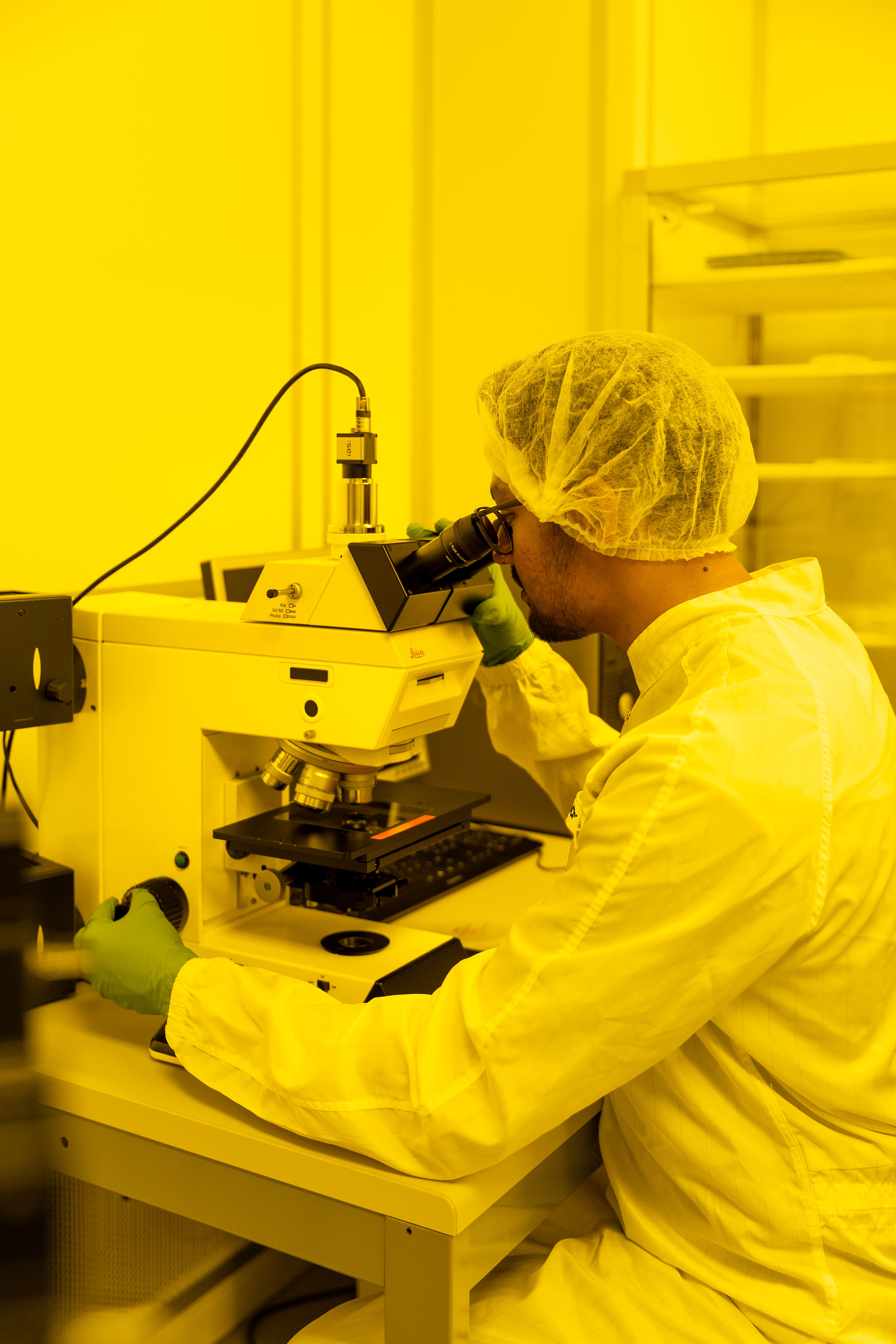
| Microscope inspectionPrüfung | – | – | – | – | – |
| 3D profile measurementsPrüfung | – | – | – | – | – |
| Cleanroom services (full photonics device processing stack)Halbleiterprozesstechnik | – | – | – | – | – |
| Collaborative engineering & co-developmentEngineering | – | – | – | – | – |
9 Anlagen & Maschinen
| Maschine | Hersteller / Modell | Anzahl | Arbeitsraum | Baujahr | Standort |
|---|---|---|---|---|---|
| Cleanroom (controlled-environment processing) | – | – | – | – | Ulm |
| Probe station (wafer/die test) | – | – | – | – | Ulm |
| Lithographie / Mask-Alignment-Anlage | – | – | – | – | Ulm |
| Metal Evaporation System | – | – | – | – | Ulm |
| Wet Bench | – | – | – | – | Ulm |
| Dicing equipment (wafer singulation) | – | – | – | – | Ulm |
| Wire bonder / Die attach equipment | – | – | – | – | Ulm |
| 3D profile measurement system | – | – | – | – | Ulm |
| Automated die tester & tape sorter | – | – | – | – | Ulm |
Zusatzleistungen
Qualität und Traceability
Jedes Bauelement wird charakterisiert und dokumentiert – mit L-I-V-Kurven, Spektren, Reliability-Stress und vollständiger Lot-Dokumentation. Die Small-Volume-Production umfasst Prozess-Lock, Qualifikation, SPC und.full Lot-Traceability auf Qualitätsniveau der Hochvolumenfertigung.
| Nachweis | Ulm |
|---|---|
| Lot traceability & SPC | |
| Reliability stress testing | |
| ISO 9001 |