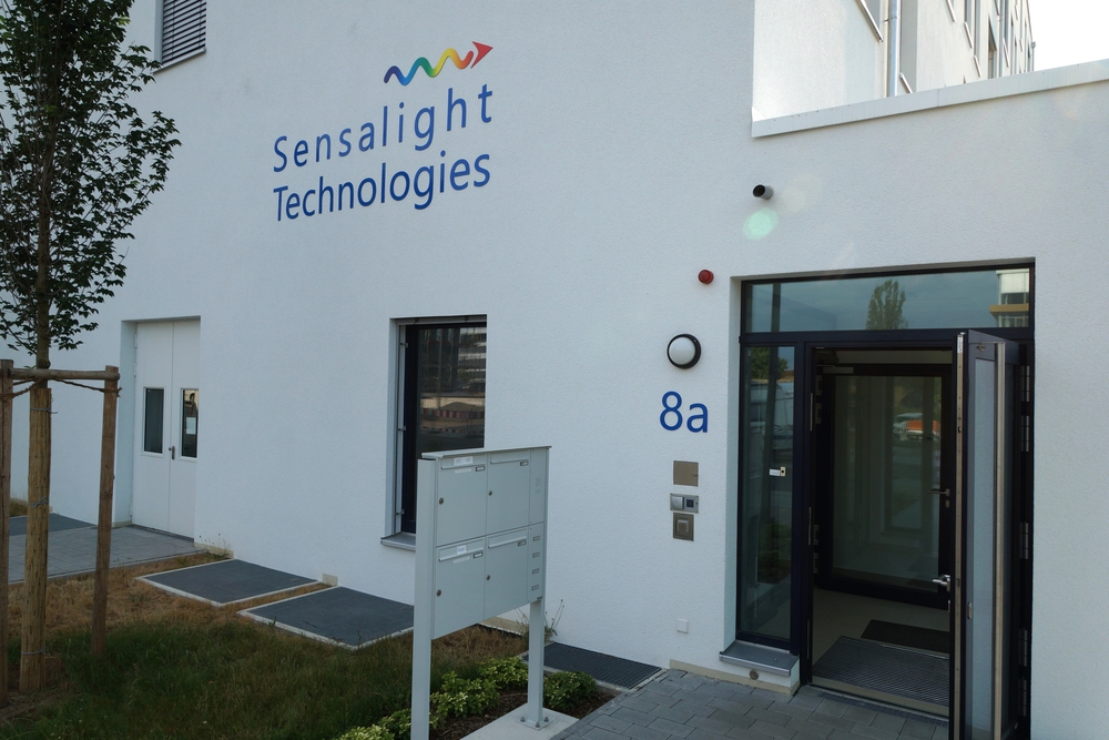
Development and manufacture of semiconductor lasers and LEDs for gas, liquid and solid analysis in sensing applications

Sensalight Technologies GmbH
WürzburgNew on Amplifa
About Sensalight Technologies
Sensalight Technologies GmbH develops and manufactures semiconductor lasers and laser systems in Würzburg for real-time analysis of gases, liquids and solid materials. The product portfolio comprises distributed-feedback lasers (DFB) for gas sensing, widely tunable monolithic coupled-cavity lasers for liquid and solid measurements, and mid-infrared LEDs with wavelengths between 2,800 and 6,500 nm based on interband cascade heterostructures. Laser specifications are customer-specific and adjustable from below 1 µm to beyond 10 µm. As a vertically integrated company, Sensalight covers the entire technology chain from laser design through epitaxy and nanofabrication to characterization and assembly. In addition, the company offers technology services including electron-beam lithography with feature sizes of around 10 nm, optical lithography, wet and dry etching, as well as dielectric and metallic coating by evaporation and sputtering on wafers up to 8 inches. Applications are found in environmental and climate monitoring, medical diagnostics, security technology, automotive and industrial process control.
- Site
- Würzburg
- Processes
- Semiconductor laser manufacturing (design to assembly, vertically integrated), Nanofabrication via electron-beam lithography, Optical lithography, Dry etching, Wet etching, Dielectric and metallic coating by evaporation, Coating by sputtering, Laser characterization and testing
- Materials
- GaAs, InP, GaSb, Gallium arsenide (GaAs), Indium phosphide (InP), Gallium antimonide (GaSb), Electron-beam lithography, Wet and dry etching
- Certificates
- DIN EN ISO 9001:2015, ISO 9001
- Founded
- 2019
- Employees
- 45
- Industries
- Environmental and climate monitoring, Medical technology, Security technology, Automotive, Industrial process control, Environmental/climate monitoring
- 01
Design and Development
- 02
Molecular Beam Epitaxy
- 03
Electron-Beam and Optical Lithography
- 04
Wet and Dry Etching
- 05
Coating (Evaporation, Sputtering)
- 06
Laser Characterization and Testing
- 07
Assembly and Sales
Materials and Processes
Gallium arsenide (GaAs)
III-V semiconductor substrate for DFB and tunable sensing lasers in the shorter wavelength range.
Indium phosphide (InP)
Substrate material for single-mode lasers in the near- and mid-infrared range.
Gallium antimonide (GaSb)
Basis for mid-IR LEDs and lasers with wavelengths up to beyond 10 µm.
Electron-beam lithography
Nanofabrication with feature sizes down to approx. 10 nm on wafers up to 8 inches.
Wet and dry etching
Structuring of wafers up to 8 inches for laser fabrication.
Evaporation and sputtering
Dielectric and metallic coating of wafers up to 8 inches.
Locations
Würzburg
DEHeadquarters: Development, Manufacturing, Characterization, Sales
- Materials
- GaAs, InP, GaSb
- 700 m² cleanroom with complete laser production line
- Electron-beam lithography system (wafers up to 6")
- Evaporation coating system (wafers up to 8")
- Sputtering system (wafers up to 8")
- Etching systems, wet and dry (wafers up to 8")
- Optical and electron microscope for inspection
Products and Components
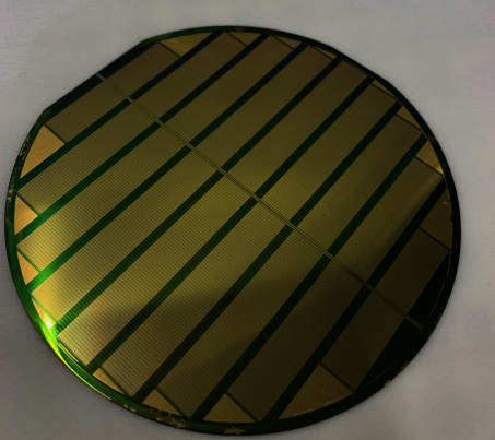
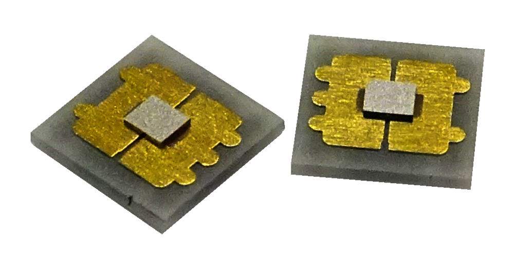
Inside the production
Industries
Processes & technical limits
| Processes | Tolerance | Max. part | Weight | Lot size | Materials |
|---|---|---|---|---|---|
| Semiconductor laser manufacturing (design to assembly, vertically integrated)Additive | – | – | – | – | GaAs, InP, GaSb |
| Nanofabrication via electron-beam lithographyEngineering | approx. 10 nm feature size | wafers up to 6" × wafers up to 6" | – | – | GaAs, InP, GaSb |
| Optical lithographyEngineering | – | wafers up to 8" × wafers up to 8" | – | – | GaAs, InP, GaSb |
| Dry etchingSurface | – | wafers up to 8" × wafers up to 8" | – | – | GaAs, InP, GaSb |
| Wet etchingSurface | – | wafers up to 8" × wafers up to 8" | – | – | GaAs, InP, GaSb |
| Dielectric and metallic coating by evaporationSurface | – | wafers up to 8" × wafers up to 8" | – | – | GaAs, InP, GaSb |
| Coating by sputteringSurface | – | wafers up to 8" × wafers up to 8" | – | – | GaAs, InP, GaSb |
| Laser characterization and testingTesting | – | – | – | – | GaAs, InP, GaSb |
| Manufacture of distributed-feedback lasers (DFB)Additive | – | – | – | – | GaAs, InP, GaSb |
| Manufacture of widely tunable monolithic lasers (coupled cavity)Additive | – | – | – | – | GaAs, InP, GaSb |
| Manufacture of mid-IR LEDs (interband cascade heterostructures)Additive | – | – | – | – | GaSb |
| Molecular beam epitaxy (MBE)Casting | – | – | – | – | GaAs, InP, GaSb |
6 Anlagen & Maschinen
| Machine | Manufacturer / model | Quantity | Working area | Year built | Site |
|---|---|---|---|---|---|
| Electron-beam lithography system | – | – | wafers up to 6" | – | Würzburg |
| Evaporation coating system | – | – | wafers up to 8" | – | Würzburg |
| Sputtering system | – | – | wafers up to 8" | – | Würzburg |
| Etching systems (wet and dry) | – | – | wafers up to 8" | – | Würzburg |
| Optical and electron microscope (inspection) | – | – | – | – | Würzburg |
| Cleanroom (700 m²) with complete laser production line | – | 1 | 700 m² | 2022 | Würzburg |
Additional services
Quality
The quality management system is certified to DIN EN ISO 9001:2015 by All-Cert (certificate no. 301671, valid until 21.11.2025). Optical and electron microscopes as well as characterization and test setups for laser manufacturing are available for inspection.
| Evidence | Würzburg |
|---|---|
| ISO 9001 |
History
- 2019
Founding of Sensalight Technologies by Alfred Forchel and Johannes Koeth as a spin-off from semiconductor laser research in Würzburg; both had already founded nanoplus Nanosystems and Technologies in 1998.
- 2022
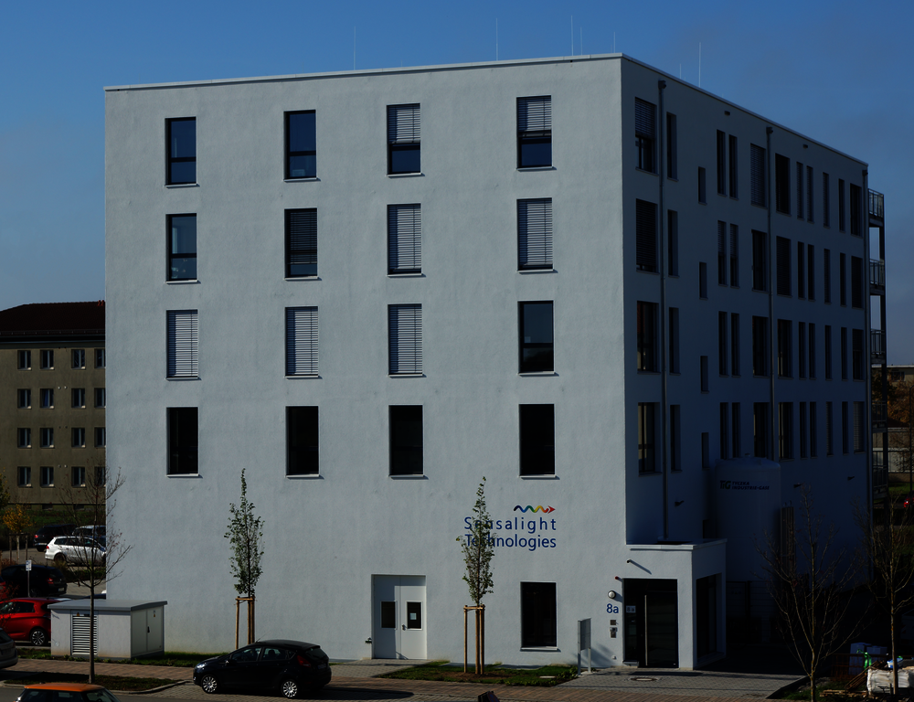
Move to new premises with a 700 m² cleanroom and complete laser production line.