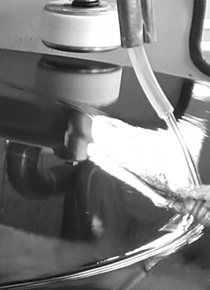
Supplier of silicon, glass and specialty wafers with in-house grinding and polishing production as well as wafer services from Aachen

SIEGERT WAFER GmbH
Aachen (DE)New on Amplifa
About SIEGERT WAFER
SIEGERT WAFER GmbH from Aachen supplies universities, research laboratories and industry with wafers and substrates. The portfolio includes silicon wafers, substrates made of fused silica, Borofloat and other glasses, sapphire, SOI and silicon carbide as well as mask blanks, complemented by specialty materials such as germanium, III/V compound semiconductors (GaAs, InP and others), lithium niobate and single-crystal quartz. In addition to trading, the company operates its own grinding and polishing production for customer-owned or supplied wafers, including backgrinding, CMP polishing, reclaim and special grinding services such as pocket wafers. Further services include dicing, laser processing, coatings (PVD, CVD, thermal oxide, nitride, ITO) as well as metrology with SEM, AFM and ellipsometry. Thanks to a large warehouse, the company can deliver at short notice and also separate individual wafers from stock. SIEGERT WAFER coordinates external process steps as one-stop support through a network of specialized partners.
- Site
- Aachen
- Processes
- Wafer Grinding / Backgrinding (Wafer Thinning), Polishing (CMP stock polish and final polish), Reclaim (silicon wafers only), Special Grinding Services (e.g. adapter pockets, pocket wafers), Dicing (cutting wafers into chips), Laser Processing (scribing, marking, cutting), Coatings / Metallization (PVD, CVD, Electroplating, Evaporating), Thermal Oxide (Dry/Wet), LTO, TEOS SiO2
- Materials
- Silicon (Si), Fused Silica, Borofloat, Glass (general), Sapphire, SOI (Silicon on Insulator), Silicon Carbide, Germanium
- Certificates
- ISO 9001:2015, ISO 9001, IATF 16949
- Industries
- Semiconductor industry, Universities and research laboratories, Microsystems technology/nanotechnology
- 01
Procurement and warehousing of wafers and substrates
- 02
Grinding and polishing in in-house production
- 03
Dicing and laser processing
- 04
Coatings and thermal oxidation
- 05
Metrology and quality inspection
- 06
Shipping and coordination of external process steps
Location
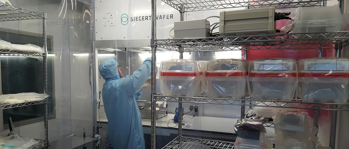
Aachen
DEHeadquarters with warehouse and in-house grinding and polishing production
- Lot size
- Single wafers to series
- Materials
- Silicon, glass, sapphire, SOI, silicon carbide and more
- Wafer geometry measuring device E&H MX-204
- Film thickness measuring device Filmetrics F50-NIR
- Scanning electron microscope (SEM)
- Atomic force microscope (AFM)
- Ellipsometer
Wafers & Substrates
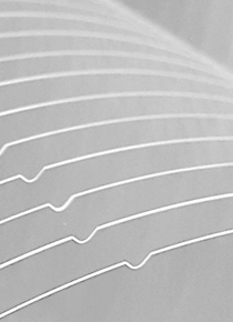
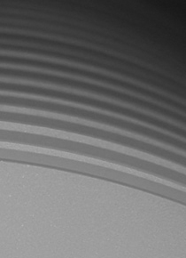
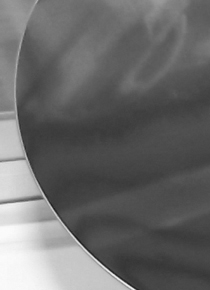
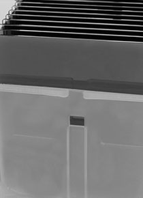
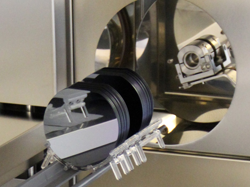
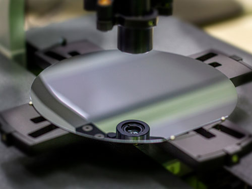
Inside the production
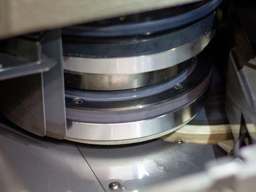
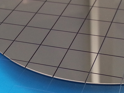
Industries
Processes & technical limits
| Processes | Tolerance | Max. part | Weight | Lot size | Materials |
|---|---|---|---|---|---|
| Wafer Grinding / Backgrinding (Wafer Thinning)Machining | – | – | – | – | Silicon, Glass, Quartz, Sapphire |
| Polishing (CMP stock polish and final polish)Surface | – | – | – | – | Silicon, Glass, Quartz, Sapphire |
| Reclaim (silicon wafers only)Surface | – | – | – | – | Silicon |
| Special Grinding Services (e.g. adapter pockets, pocket wafers)Machining | – | – | – | – | Silicon, Glass |
| Dicing (cutting wafers into chips)Machining | – | – | – | – | Silicon, Glass, Quartz, Sapphire |
| Laser Processing (scribing, marking, cutting)Machining | – | – | – | – | Silicon, Glass, Quartz, Sapphire |
| Coatings / Metallization (PVD, CVD, Electroplating, Evaporating)Surface | – | – | – | – | Silicon, Glass, Sapphire |
| Thermal Oxide (Dry/Wet), LTO, TEOS SiO2Surface | – | – | – | – | Silicon |
| LPCVD Nitride / PECVD Nitride, Polysilicon, Photoresist, ITO CoatingSurface | – | – | – | – | Silicon |
| SiO2 Removal from Wafer Backside (HF Dip)Surface | – | – | – | – | Silicon |
| Metrology (SEM, AFM, Type- & Resistivity-Check, Ellipsometry, Wafer Geometry, Film Thickness)Testing | – | – | – | – | Silicon, Glass, Sapphire |
| Wafer Trading and Logistics (Warehousing, Coordination of External Process Steps)Engineering | – | – | – | – | Silicon, Glass, Sapphire, SOI, Silicon Carbide |
5 Anlagen & Maschinen
| Machine | Manufacturer / model | Quantity | Working area | Year built | Site |
|---|---|---|---|---|---|
| Wafer geometry measuring device | E&H MX-204 | – | – | – | Aachen |
| Film thickness measuring device | Filmetrics F50-NIR | – | – | – | Aachen |
| Scanning electron microscope (SEM) | – | – | – | – | Aachen |
| Atomic force microscope (AFM) | – | – | – | – | Aachen |
| Ellipsometer | – | – | – | – | Aachen |
Additional services
Quality
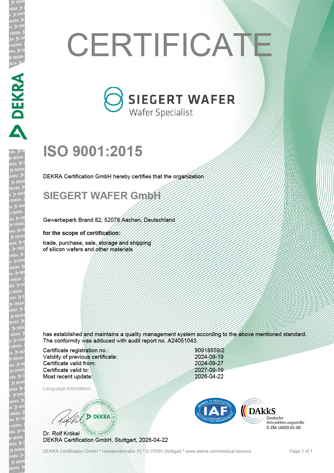
Quality is ensured by a quality management system certified according to ISO 9001:2015 (DEKRA, No. 90918559/2). Metrology includes SEM, AFM, type and resistivity checks, ellipsometry, wafer geometry (E&H MX-204) and film thickness measurement (Filmetrics F50-NIR).
| Evidence | Aachen |
|---|---|
| ISO 9001 | |
| IATF 16949 |