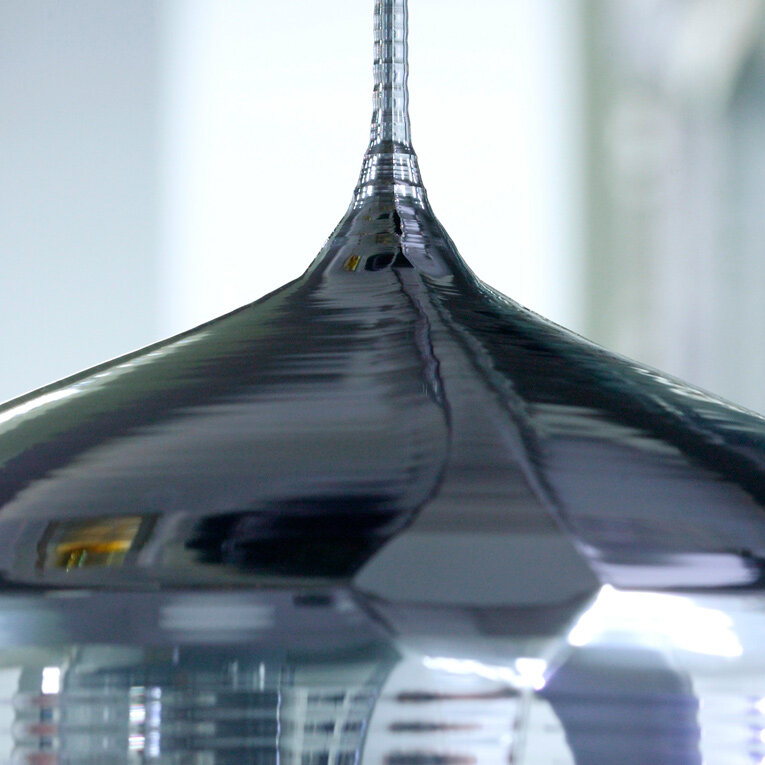
Siltronic manufactures high-tech silicon wafers up to 300 mm in diameter as the base material for semiconductor chips worldwide.

Siltronic AG
Munich · Burghausen · Freiberg · Singapore · Portland, ORNew on Amplifa
About Siltronic
Siltronic AG, headquartered in Munich, is a manufacturer of wafers made from hyperpure silicon and supplies semiconductor manufacturers all over the world. The company produces polished and epitaxial wafers as well as sawn, etched and lapped wafers with diameters from 200 mm to 300 mm. Production encompasses hyperpure silicon and polysilicon manufacturing, crystal growing using the Czochralski and float zone processes, and doping with boron, phosphorus, antimony and arsenic. Customers include among others the twenty world-leading companies of the semiconductor industry, for whom Siltronic acts as a strategic development partner; the innovative strength is evidenced by almost 2,000 patents and patent applications. Production takes place in a global network of plants in Europe, Asia and the USA, including Europe's largest 300-mm fab in Freiberg and the modern 300-mm fab opened in Singapore in 2024. The company employs around 4,300 people and has been listed in the Prime Standard since 2015.
- Site
- München
- Processes
- Wafer manufacturing (silicon wafers, diameters up to 300 mm), Czochralski crystal growing (Cz method), Float zone process (Float Zone), Manufacture of polished wafers (polished wafers), Manufacture of epi wafers (epitaxially deposited layers), Sawing of wafers (as cut), Etching of wafers (etched surface), Lapping of wafers (lapped surface)
- Materials
- Hyperpure silicon / hyperpure silicon, Polysilicon, Silicon (monocrystalline), Doping boron, Doping phosphorus, Doping antimony, Doping arsenic, Hyperpure silicon / polysilicon
- Certificates
- IATF 16949, DIN EN ISO 14001, DIN EN ISO 9001, ISO 45001, ISO 50001, ISO/IEC 27001, ISO 9001, ISO 14001
- Founded
- 1953
- Employees
- 4300
- Industries
- Semiconductor industry, Semiconductor chip manufacturers
- 01
Hyperpure silicon / polysilicon production
- 02
Crystal growing (Czochralski / Float Zone)
- 03
Doping (B, P, Sb, As)
- 04
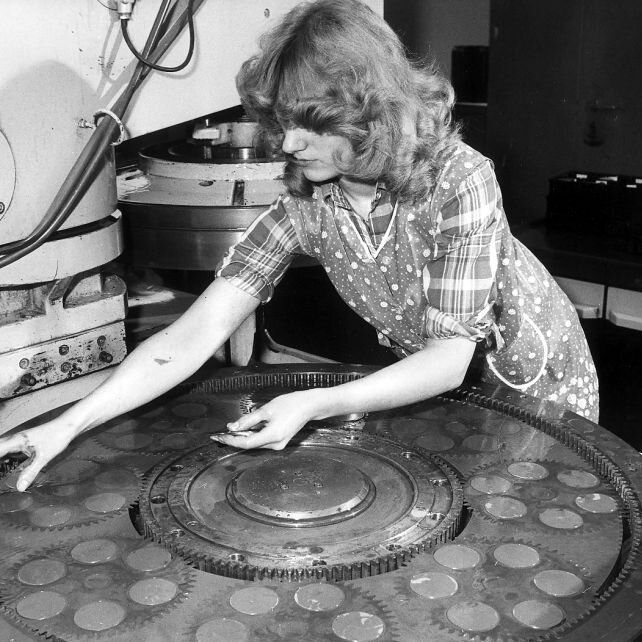
Sawing
- 05
Lapping
- 06
Etching
- 07
Polishing
- 08
Epitaxy
- 09
Quality inspection
- 10
Worldwide distribution
Materials and Processes
Hyperpure silicon / polysilicon
Base raw material for monocrystals and silicon wafers up to 300 mm in diameter.
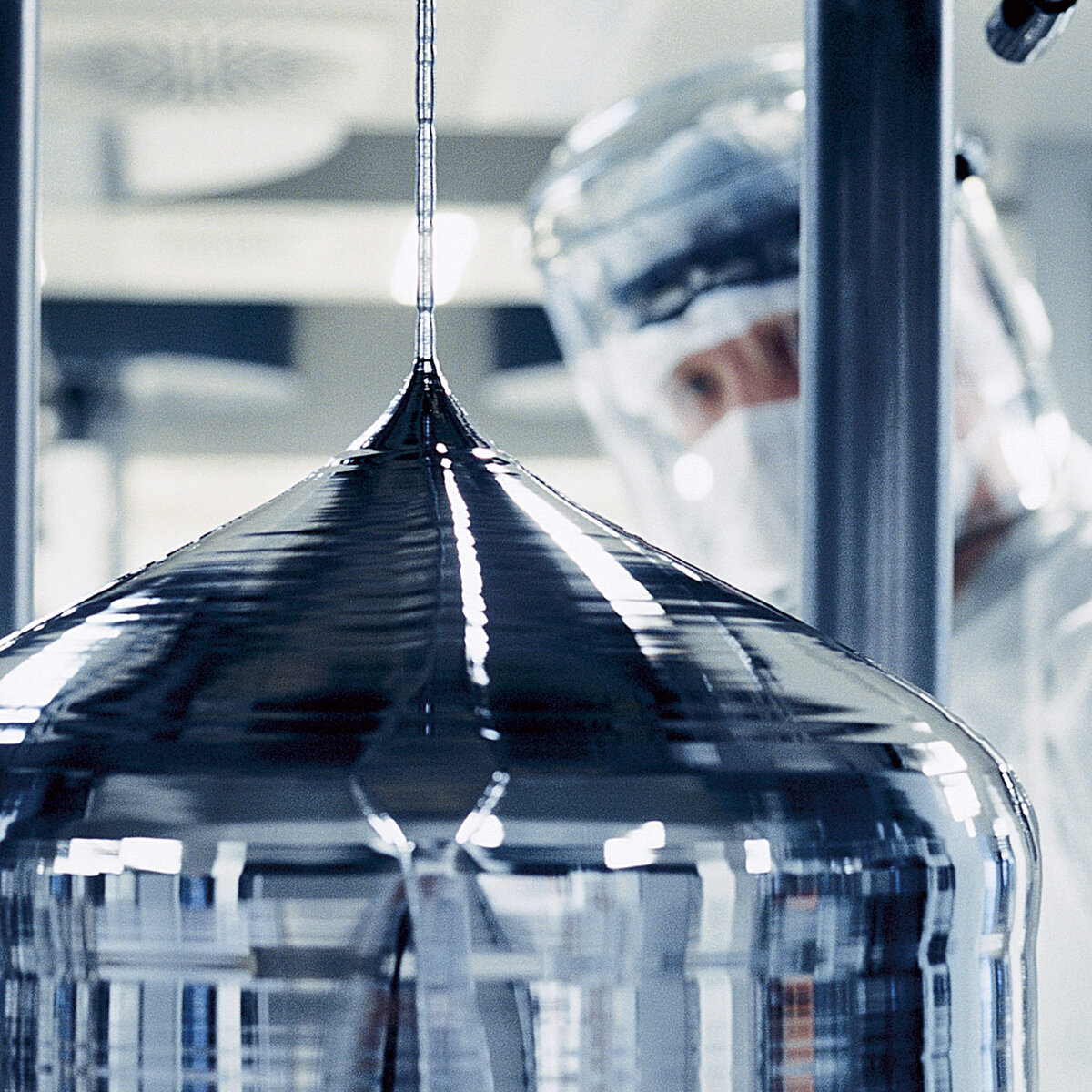
Czochralski process
Crystal growing of monocrystalline silicon ingots for the majority of wafer production.
Float zone process (Float Zone)
Growing process for wafers with particularly high purity requirements, in use since 1959.
Doping (boron, phosphorus, antimony, arsenic)
Targeted doping of the wafers to set the electrical conductivity.
Epitaxy
Deposition of epitaxial layers on polished wafers for demanding applications.
Locations
Munich
DEHeadquarters
Burghausen
DEProduction, central R&D; hyperpure silicon and wafers up to 300 mm
- Materials
- Hyperpure silicon, silicon wafers up to 300 mm
- Float zone crystal growing system (Float Zone, since 1959)
- 300-mm pilot production line (from 1998)
Freiberg
DEProduction; largest 300-mm fab in Europe
- Materials
- Silicon (monocrystalline)
- 300-mm silicon wafer fabrication plant (production start 2004)
Singapore
SGProduction (200/300 mm)
- Materials
- Silicon (monocrystalline)
- Production facilities for 200 mm and 300 mm wafers
- New 300-mm fab (opened 2024)
Portland, OR
USProduction (200 mm)
- Materials
- Silicon (monocrystalline)
Products
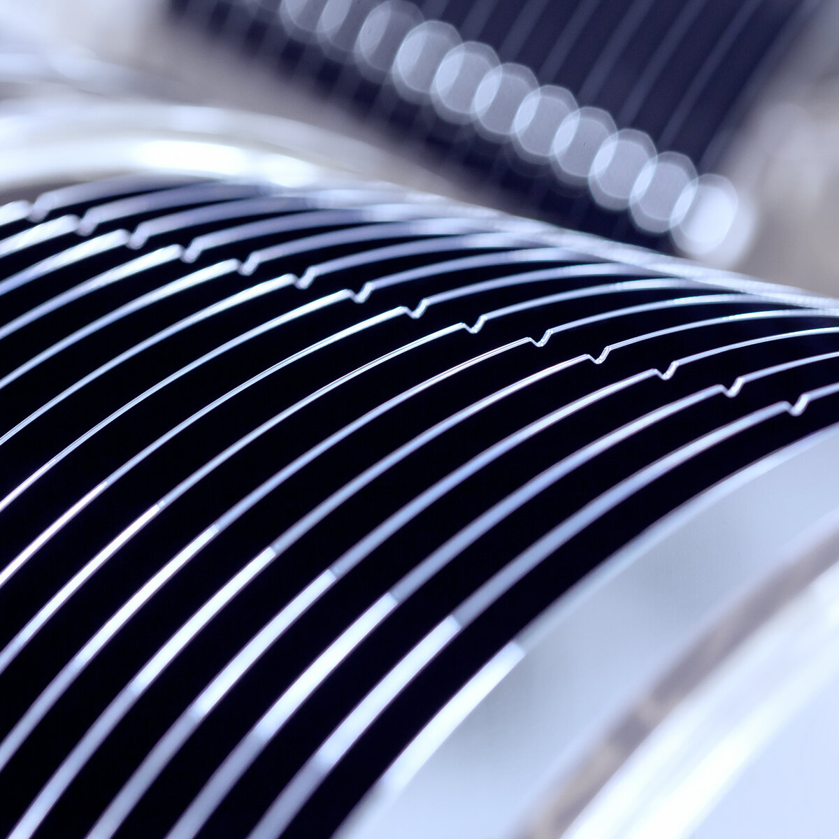
Inside the production

Industries
Processes & technical limits
| Processes | Tolerance | Max. part | Weight | Lot size | Materials |
|---|---|---|---|---|---|
| Wafer manufacturing (silicon wafers, diameters up to 300 mm)Semiconductor/wafer manufacturing | – | 300 mm diameter | – | – | Hyperpure silicon |
| Czochralski crystal growing (Cz method)Crystal growing | – | – | – | – | Silicon |
| Float zone process (Float Zone)Crystal growing | – | – | – | – | Silicon |
| Manufacture of polished wafers (polished wafers)Surface | – | – | – | – | Hyperpure silicon |
| Manufacture of epi wafers (epitaxially deposited layers)Semiconductor/wafer manufacturing | – | – | – | – | Hyperpure silicon |
| Sawing of wafers (as cut)Machining | – | – | – | – | Silicon |
| Etching of wafers (etched surface)Surface | – | – | – | – | Silicon |
| Lapping of wafers (lapped surface)Surface | – | – | – | – | Silicon |
| Hyperpure silicon production (polysilicon)Semiconductor/wafer manufacturing | – | – | – | – | Hyperpure silicon, Polysilicon |
| Manufacture of monocrystals (ingots)Crystal growing | – | 300 mm diameter | – | – | Silicon |
| Doping of wafers (boron, phosphorus, antimony, arsenic)Semiconductor/wafer manufacturing | – | – | – | – | Silicon, Boron, Phosphorus, Antimony, Arsenic |
4 Anlagen & Maschinen
| Machine | Manufacturer / model | Quantity | Working area | Year built | Site |
|---|---|---|---|---|---|
| Float zone crystal growing system (Float Zone) | – | – | – | 1959 | Burghausen |
| 300 mm wafer fabrication plant (fab) | – | – | – | 2023/2024 | Singapore |
| 300 mm silicon wafer fabrication plant (fab) | – | – | – | 2004 | Freiberg |
| Production facilities for 200 mm and 300 mm wafers | – | – | – | – | Singapore |
Additional services
Reference customers
Quality
At all locations, Siltronic works according to the same technologies and certified standards; the integrated management system (IMS) combines quality, occupational safety, environmental protection, information and energy management.
| Evidence | Burghausen | Freiberg | Singapore | Portland, OR |
|---|---|---|---|---|
| IATF 16949 | ||||
| ISO 9001 | ||||
| ISO 14001 | ||||
| ISO 45001 | ||||
| ISO 50001 |
History
- 1953
Start of R&D in the field of hyperpure silicon
- 1958
Start of semiconductor production
- 1961
Industrial-scale hyperpure silicon production
- 1962
Development of the first silicon wafer
- 1968
Founding of Wacker-Chemitronic GmbH, Burghausen
- 1978
Founding of Wacker Siltronic Corporation, Portland (USA)
- 1984
First 200-mm wafers
- 1995
Wafer business of Wacker-Chemitronic transferred to Wacker Siltronic; acquisition of Freiberger Elektronikwerkstoffe
- 1996
Conversion into an AG (Wacker Siltronic AG)
- 1997
Founding of Wacker Siltronic Singapore Pte. Ltd.
- 1999
Production start of the Singapore fabrication plant
- 2004
Production start of the 300-mm fab in Freiberg; renamed Siltronic AG
- 2006
Founding of JV Siltronic Samsung Wafer Pte. Ltd. with Samsung; construction start of the 300-mm fab in Singapore
- 2014
Acquisition of 78% of Siltronic Silicon Wafer Pte. Ltd.
- 2015
IPO, listing in the Prime Standard, TecDAX
- 2020
Announcement of planned acquisition by GlobalWafers for EUR 3.7 billion (raised to EUR 4.4 billion in 2021)
- 2022
German federal government does not grant approval for the sale to GlobalWafers
- 2023
Production of the first 300-mm wafers in the new Singapore fab
- 2024
Opening of the new 300-mm fab in Singapore