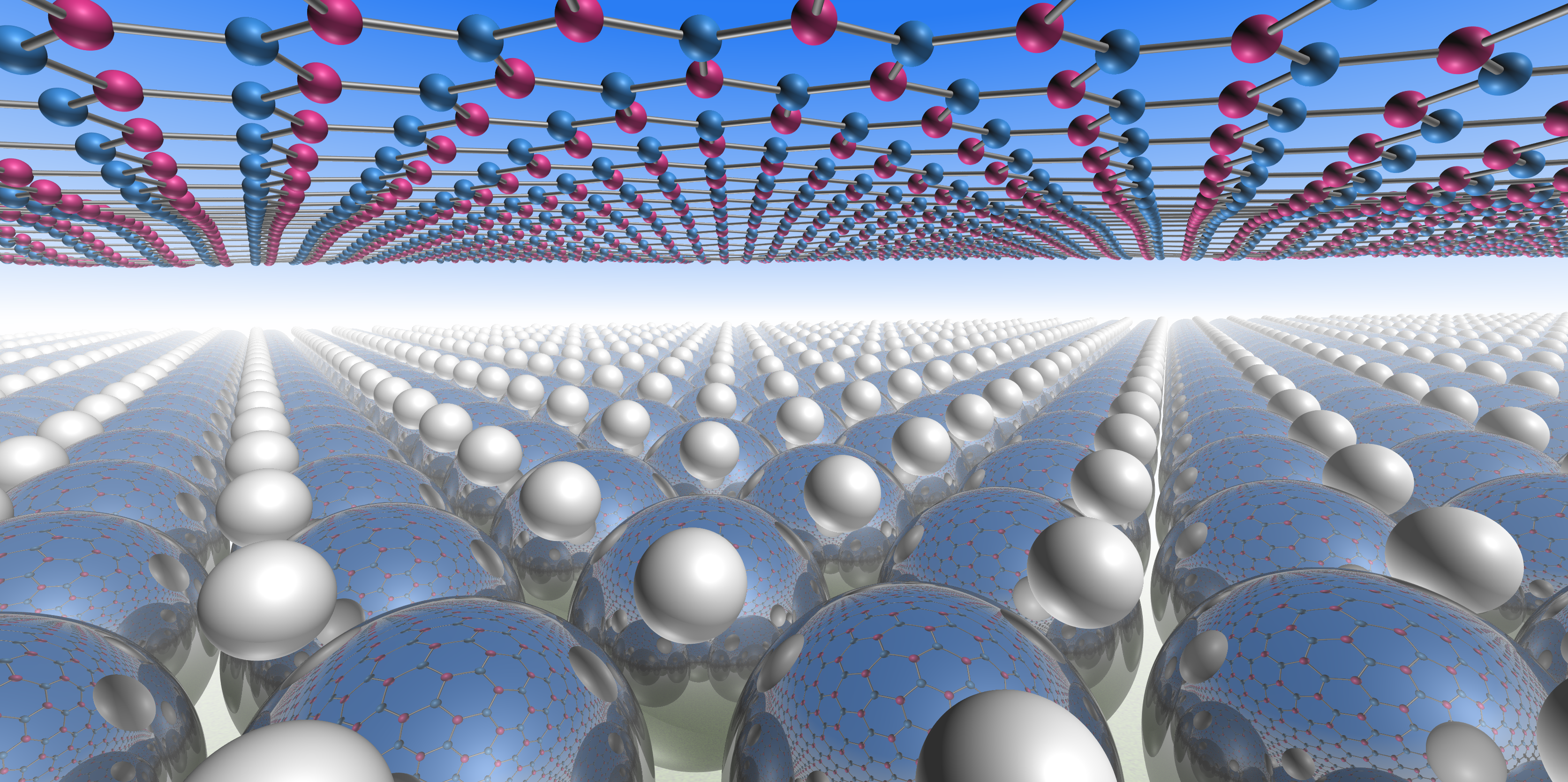
CVD synthesis of wafer-size hexagonal boron nitride (h-BN) for 2D materials applications

SwissBN.ch
Zurich (CH)New on Amplifa
About SwissBN
SwissBN is a Swiss manufacturer of 2D materials focused on hexagonal boron nitride (h-BN). The company produces high-quality, flat h-BN materials in wafer size, using chemical vapor deposition (CVD) as its core process. This unique expertise in h-BN synthesis enables ready-to-use substrates and dielectrics for applications with two-dimensional materials in semiconductor and electronics development as well as in research. SwissBN originated from the 2D Materials project of the Group for Low-Dimensional Systems at the Physics Institute of the University of Zurich and thus brings many years of scientific experience in materials synthesis and characterization. Since March 1, 2025, SwissBN has been affiliated with the Institute of Electromagnetic Fields (IEF) at ETH Zurich, strengthening its position at the interface between fundamental research and technology development in the field of advanced 2D materials.
- Site
- Zurich
- Processes
- Chemical Vapor Deposition (CVD) synthesis of hexagonal boron nitride (h-BN), CVD synthesis of hexagonal boron nitride (h-BN), Wafer-scale production of high-quality, flat 2D boron nitride materials
- Materials
- hexagonal boron nitride (h-BN), Hexagonal Boron Nitride, Chemical Vapor Deposition (CVD)
- Industries
- 2D materials, Semiconductors/Electronics, Research
- 01
Chemical vapor deposition (CVD) of h-BN synthesis
Materials and Processes
Hexagonal Boron Nitride
2D boron nitride, produced by CVD in wafer size as an insulator and dielectric material for 2D materials applications.
Chemical Vapor Deposition (CVD)
Core process for the synthesis of high-quality, flat h-BN in wafer size.
Locations
Zurich
CHManufacturing and development; since 2025 affiliated with the Institute of Electromagnetic Fields (IEF) at ETH Zurich,
- Materials
- Hexagonal boron nitride (h-BN)
- CVD systems
Materials
Inside the production
Industries
Processes & technical limits
| Processes | Tolerance | Max. part | Weight | Lot size | Materials |
|---|---|---|---|---|---|
| Chemical Vapor Deposition (CVD) synthesis of hexagonal boron nitride (h-BN)Additive | – | – | – | – | hexagonal boron nitride (h-BN) |
Additional services
History
Originated from the 2D Materials project of the Group for Low-Dimensional Systems at the Physics Institute of the University of Zurich
- 2025
Affiliated with the Institute of Electromagnetic Fields (IEF) at ETH Zurich since March 1, 2025