
Manufacturer of printed circuit boards up to 28 layers, PCB assembly, and complete electronic assemblies from a single source.

Top-Print Electronic GmbH
82054 Sauerlach (near Munich) · GermanyNew on Amplifa
About Top-Print Electronic
Top-Print Electronic GmbH is a printed circuit board manufacturer and assembler specialized in industrial electronics, based in Sauerlach near Munich. The company produces single- and double-sided PCBs as well as multilayer boards with up to 28 layers, flexible PCBs made of polyimide film from 0.05 mm thickness, and rigid-flex PCBs, including special versions such as blind vias, buried vias, microvias, and surface finishes (HAL, immersion tin, immersion gold, electroplated gold connectors). The offering is complemented by SMD and THT assembly, complete assembly manufacturing including functional testing and final inspection, laser-cut stainless steel solder paste stencils, individually punched and milled front panels, customer-specific toroidal transformers, and ultra-fine conductor traces on film in a roll-to-roll process with structures from 20 µm. Batch sizes range from prototypes with pool service through small and medium series to large series via partner companies. An express service handles urgent orders at short notice. Customers come from industrial electronics, medical technology, rail and transport engineering, aerospace, and solar technology, as well as from start-ups and design offices.
- Site
- Sauerlach
- Processes
- PCB manufacturing (single-layer to 28-layer multilayer), Flexible PCB manufacturing and assembly, Rigid-flex PCBs, Blind vias / buried vias / microvias, Surface finish: HAL (Hot Air Leveling), Surface finish: immersion tin, Surface finish: immersion gold, Electroplated gold connectors
- Materials
- Glass fiber mats (epoxy resin impregnated, base material for PCBs), Copper, Polyimide film, Stainless steel (solder paste stencils), Brass (stencil material), Polymer (stencil material), PET film, PEN film
- Certificates
- AOI (Automated Optical Inspection), Functional testing and final inspection, Electrical tests and degradation tests (ultra-fine conductor traces), RF measurements up to 100 GHz
- Founded
- 2000
- Industries
- Industrial electronics, Medical technology, Rail and transport engineering, Aerospace technology, Solar technology, Start-ups and design offices
- 01
PCB unbundling including circuit unbundling and Gerber data creation
- 02
Component procurement
- 03
PCB manufacturing (single-layer to 28 layers, flexible, rigid-flex)
- 04
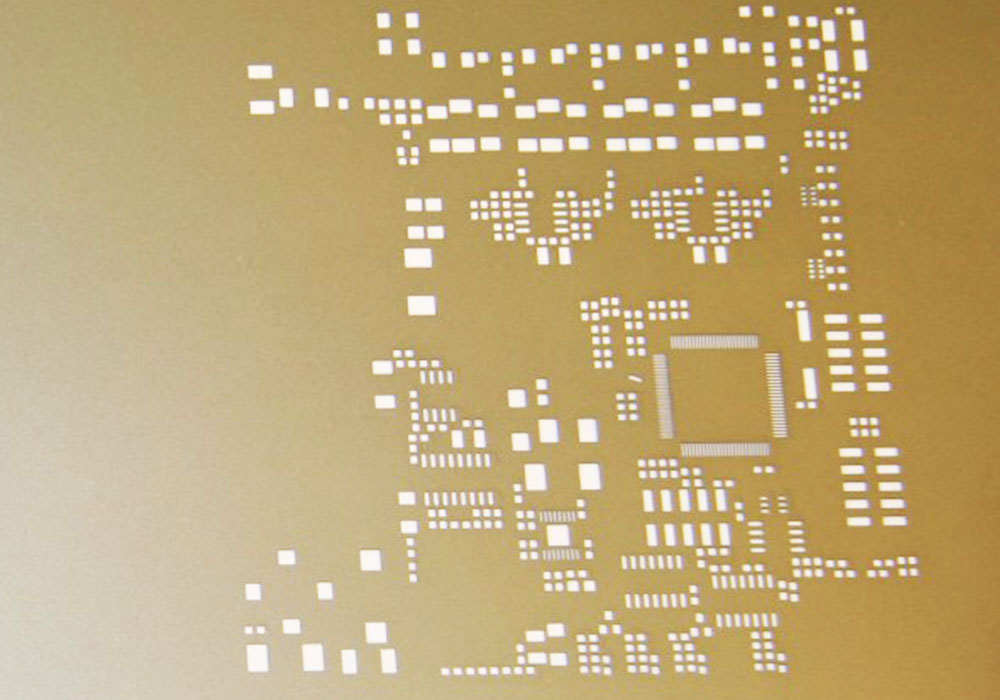
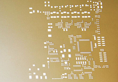
Solder paste stencil manufacturing (laser-cut)
- 05
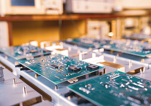
SMD and THT assembly
- 06
Reflow, wave, and selective soldering
- 07
Functional testing and final inspection
Materials & Processes
Glass fiber mats with epoxy resin
Base material for rigid PCBs due to good tracking resistance.
Copper
Conductive layer for traces, windings, and thin-film metallization.
Polyimide film
Base material for flexible PCBs from 0.05 mm thickness.
PET and PEN film
Film materials for ultra-fine conductor traces in the roll-to-roll process.
Stainless steel
Standard material for laser-cut solder paste stencils (0.02 to 0.60 mm).
Brass
Alternative stencil material for solder paste printing.
Chromium
Adhesion layer in the sputter process of Cu thin-film metallization.
Ferromagnetic sheet metal (iron)
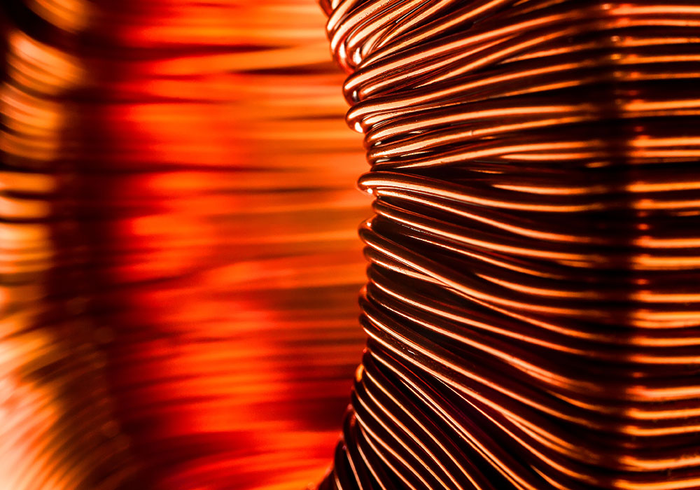
Toroidal core made of wound sheet metal for customer-specific toroidal transformers.
Location
Sauerlach
DECompany headquarters with production
- Lot size
- Prototypes to large series
- Materials
- FR4, copper, polyimide, stainless steel
- Automated SMD assembly lines
- AOI (Automated Optical Inspection)
- Laser system for stencil manufacturing
- Punching and milling technology
- Film web systems (roll-to-roll, 215 mm web width)
- Sputtering system (Cu thin-film metallization)
Components
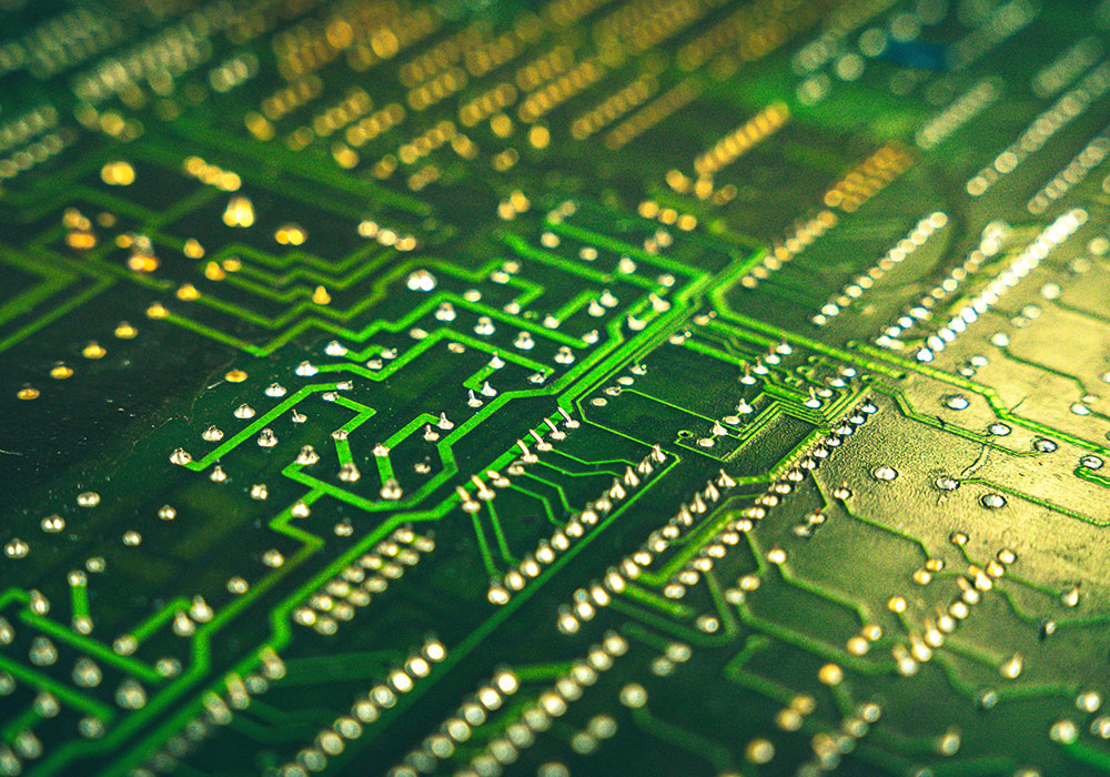
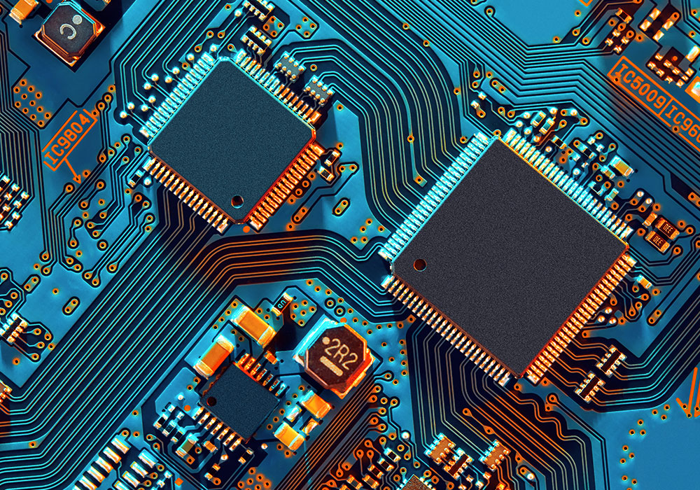
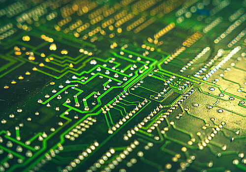
Inside the production
Industries
Processes & technical limits
| Processes | Tolerance | Max. part | Weight | Lot size | Materials |
|---|---|---|---|---|---|
| PCB manufacturing (single-layer to 28-layer multilayer)Printed circuit boards | – | – | – | Prototype (pool service) – Large series | FR4/glass fiber mats with epoxy resin, Copper |
| Flexible PCB manufacturing and assemblyPrinted circuit boards | – | – | – | Small series – Large series | Polyimide film (from 0.05 mm thickness) |
| Rigid-flex PCBsPrinted circuit boards | – | – | – | – | Polyimide film, Glass-fiber-reinforced epoxy resin |
| Blind vias / buried vias / microviasPrinted circuit boards | – | – | – | – | – |
| Surface finish: HAL (Hot Air Leveling)Surface | – | – | – | – | Printed circuit boards |
| Surface finish: immersion tinSurface | – | – | – | – | Printed circuit boards |
| Surface finish: immersion goldSurface | – | – | – | – | Printed circuit boards |
| Electroplated gold connectorsSurface | – | – | – | – | Printed circuit boards |
| SMD assembly (Surface Mount Device)Assembly | – | – | – | Prototypes/single pieces – Large series | – |
| THT assembly (Through Hole Technology)Assembly | – | – | – | Single pieces | – |
| Reflow solderingJoining | – | – | – | – | – |
| Wave solderingJoining | – | – | – | – | – |
| Selective solderingJoining | – | – | – | – | – |
| Assembly manufacturing incl. functional testing and final inspectionAssembly | – | – | – | – | – |
| Solder paste stencil manufacturing (laser-cut)Printed circuit boards | – | – | – | – | Stainless steel, Brass, Polymer |
| PCB unbundling including circuit unbundling and Gerber data creationEngineering | – | – | – | – | – |
| Component procurement (active/passive components)Engineering | – | – | – | – | – |
| Front panel manufacturing (punching and milling technology)Machining | – | – | – | very high volumes | – |
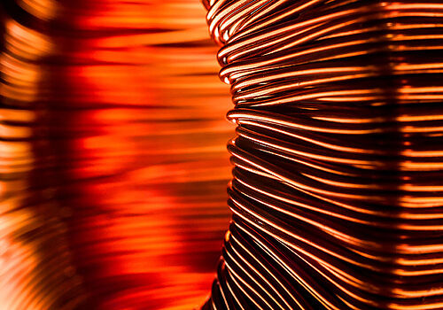
| Toroidal transformer manufacturing (customer-specific)Assembly | – | – | – | – | Copper (winding), ferromagnetic sheet metal (iron ring) |
| Ultra-fine conductor traces on film (roll-to-roll, lithography, min. structure 20 µm)Printed circuit boards | – | 100 m (film length, typ. approx. 20 m) × 215 mm | – | – | PET, PEN, Polyimide, Copper, Chromium (adhesion layer) |
| Cu thin-film metallization (sputter process, ≤ 1.0 µm)Surface | – | 215 mm | – | – | Copper, Chromium |
| Semi-additive Cu metallization (pattern plating up to approx. 10 µm)Surface | – | 215 mm | – | – | Copper |
| Screen printing (dielectric/conductive functional materials, 10-20 µm)Surface | – | 215 mm | – | – | Electroluminescent functional materials |
| Laser processing (structuring, vias, contour cutting)Machining | – | 215 mm | – | – | Films |
| Laminating (protective films, full-surface)Joining | – | 215 mm | – | – | Protective films |
| Testing and characterization (AOI, electrical tests, degradation tests, RF up to 100 GHz)Testing | – | – | – | – | – |
| Circuit development / CAD servicesEngineering | – | – | – | – | – |
7 Anlagen & Maschinen
| Machine | Manufacturer / model | Quantity | Working area | Year built | Site |
|---|---|---|---|---|---|
| Automated SMD assembly lines | – | – | – | – | Sauerlach |
| Laser system for stencil manufacturing (laser technology) | – | – | – | – | Sauerlach |
| Punching technology | – | – | – | – | Sauerlach |
| Milling technology | – | – | – | – | Sauerlach |
| AOI (Automated Optical Inspection) | – | – | – | – | Sauerlach |
| Film web systems (roll-to-roll, 215 mm web width, process area approx. 185 × 185 mm) | – | – | Grid 200 mm, active process area approx. 185 * 185 mm, partial processes on rigid substrates ≤ 200 | – | Sauerlach |
| Sputtering system (Cu thin-film metallization) | – | – | – | – | – |
Additional services
Quality
Assembly manufacturing includes functional testing and final inspection; assembly is carried out with automated optical inspection (AOI) and documented processes for traceability. For ultra-fine conductor traces, optical structure measurement, electrical tests, degradation tests, and RF measurements up to 100 GHz are performed.
| Evidence | Sauerlach |
|---|---|
| AOI (Automated Optical Inspection) | |
| Functional testing and final inspection | |
| Electrical tests and degradation tests (ultra-fine conductor traces) | |
| RF measurements up to 100 GHz |
History
- 2000
Founding of Top-Print Electronic GmbH in Ottobrunn.
- 2025
Relocation from Ottobrunn to Sauerlach, Robert-Bosch-Str. 14 (from 01.04.2025).